Affiliate Disclosure: This post may include affiliate links. If you click and make a purchase, I may earn a small commission at no extra cost to you.
Both charge trap flash and floating gate are non-volatile memory technologies used in flash storage devices. Essentially, these two technologies illustrate how the memory cell within the flash memory stores data in the form of charge. The charge trap is a more advanced method with better capabilities for data retention. The floating gate technology is somewhat older and is currently considered obsolete in modern SSDs.
The primary difference between these storage technologies lies in how a single storage cell retains the charge. The way of keeping the charge plays a vital role in data retention. So, there is no serious advantage in terms of performance with any of these. However, charge trap flash is better at retaining the charge and less prone to leakage.

Use-cases of CTF and FG
Floating Gate (FG) Flash use cases
The primary application of the FG Flash is in the 2D NAND flash and NOR Flash storage. Traditional solid-state drives use floating gate transistors as the storage medium. You can still find some older, low-end SSDs with floating-gate technology. Because the FG technology is cost-effective and has dominated the SSD market, it has gained a reputation in the market.
Charge Trap Flash (CTF) use cases
CTF is primarily used when storage density is critical. It is mainly used in 3D NAND technology for both consumer and enterprise storage devices. Additionally, it is utilized in data centers, cloud storage, AI processing, and in nearly every environment where endurance is crucial. Almost all modern SSDs use the CTF design instead of the floating gate.
In most high-end and flagship smartphones and tablets, you will find the CTF memory used as the primary storage. Additionally, in emerging technologies such as AI and IoT, as well as in automotive storage, the CTF is utilized. Although CTF has found its application in many areas, it is still prevalent in high-end devices, including smartphones and NVMe SSDs. There is a lot of room for scalability, and we may find this flash at cheap prices as well.
Difference in Working
The way the CTF and FG store the data differs slightly. The difference lies in how a single memory cell retains the charge. CTF is better in terms of data retention as compared to the FG. This is because of the way the CTF stores the charge. Let’s discuss how.
Floating Gate Transistor Working
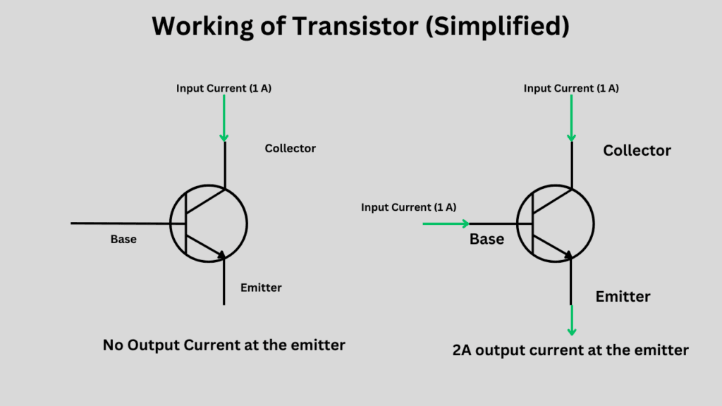
The floating gate transistor is an advanced version of the normal BJT or Transistor. A simple transistor can be used as a switch or an amplifier, provided it is set up in a proper circuit. The normal transistor allows current to flow through its two terminals (collector to emitter) when a voltage is applied to its gate. It works like in the image.
The floating gate transistor features three additional layers between the gate and the main body. One layer is the conductive floating gate, and two extra oxide layers cover the floating gate. The oxide layer acts as an insulator, holding any charge within the conductive floating gate. A floating gate is called floating because it is a conductor isolated from the main circuitry and remains floating, depending on the control gate and transistor channel.
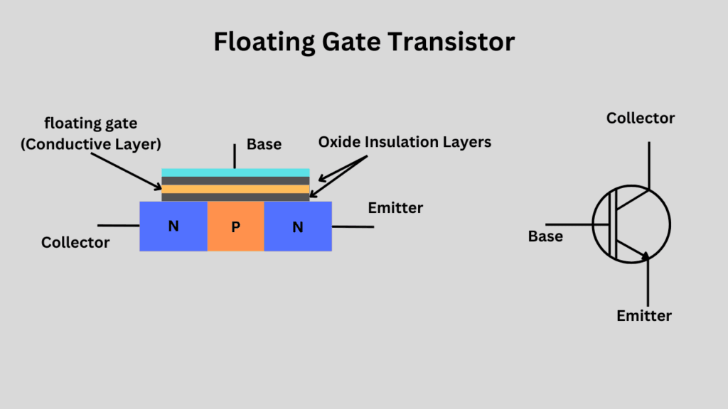
How the charge is pushed inside the floating gate is the process of writing the data in the FG-based memory. Depending on the number of bits stored inside a cell, a specific amount of charge is pushed by the controller in your SSDs or other storage devices. Once the charge is gone, the oxide layer would keep this charge from leaking out. In this way, the data is kept in its place even without the need for power.
But, over time, the floating gate leads the charge because it is stored in a conductive layer, which is prone to leakage. The oxide layer surrounding the floating gate degrades over time, resulting in increased leakage. All in all, the floating gate has no inherent properties to retain the charge on its own. It just depends on the oxide layer for holding the charge.
Charge Trap Flash Working
In the charge trap flash, everything remains the same, but the floating gate, which was a conductor, is replaced by a non-conductive or doped polycrystalline silicone. Now, we can’t call this a floating gate because the charge isn’t stored in a single continuous layer. The term “charge trap” is used because the charge is now trapped in different locations inside a dielectric material (as opposed to being free to float in the conductive layer). The charge is now stored in isolated pockets in a non-conductive material; it is called a “trap” instead of a “float”.

This simple difference in how the charge is held in place plays an important role in the overall reliability of the stored data. The total P/E cycles in the CTF are higher than those in the FG. Additionally, the error rates are lower because the likelihood of data leakage is reduced in the CTF.
Because the charge is stored in discrete and isolated trapping locations on a non-conductive material, the chances of leakage are very low. Even though the oxide layer is present here as well, the dielectric trap layer has the properties to keep the charge in place.
2D NAND vs 3D NAND
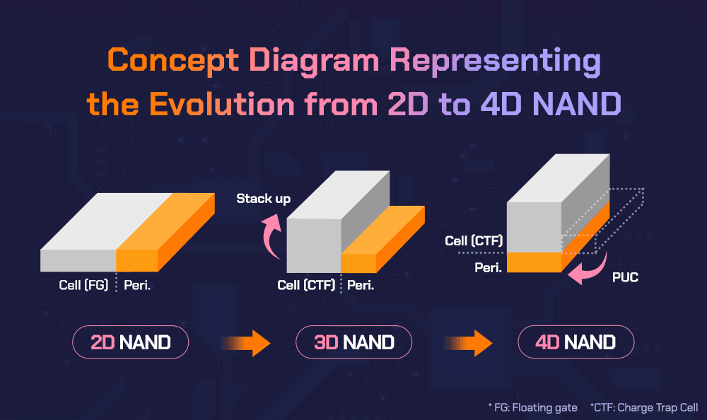
It isn’t that the 3D NAND only uses the charge trap flash. Although the current 3D NAND technology utilizes the charge trap, early deployments were initially made with Floating Gate NAND flash. I believe it is essential to understand the difference between 2D NAND and 3D NAND to grasp this concept more effectively.
2D NAND is a simple deployment of the floating gate transistors on a single plane. Although 2D NAND is well-established due to its mature technology, it has some drawbacks. Mainly, there are storage density limitations. Additionally, scalability is more challenging because the cell size can’t be reduced too much. That is why companies have started to invest in 3D NAND, and now 4D NAND is also under development.
The manufacturers have attempted to reduce the cell size to smaller process nodes (below 20 nm). But shrinking cells caused problems like cell-to-cell interference, charge retention issues, and reduced endurance. However, 2D NAND is still found in older or more cost-sensitive storage devices such as basic USB drives, SD cards, and some low-end SSDs.
In 3D NAND, memory cells are stacked vertically in multiple layers (often referred to as vertical stacking). This allows more storage capacity without shrinking the size of each cell. This creates a tower-like structure from the layers. 3D NAND offers better scalability because manufacturers can add more layers to increase density instead of shrinking the cells.
With the help of 3D NAND Flash, we get higher capacity, lower cost per gigabyte, better endurance, and improved performance over 2D NAND. 3D NAND can have 100+ layers. However, 3D NAND is complex and costly to manufacture, though advancements are continually improving yields and reducing costs.
3D NAND flash is found in modern SSDs, smartphones, high-capacity USB drives, and enterprise storage. Samsung has its marketing term for the 3D NAND, i.e., V-NAND (Vertical NAND).
Do all modern SSDs and storage devices use CTF?
No, charge trap flash is used only in high-end storage devices like the modern NVMe SSDs, expensive smartphones, etc. Brands like Samsung, Crucial, WD, etc, use the CTF in their 3D NAND products. Traditional 2D NAND is less common in the latest designs, but it can still be found in some drives, particularly the slower and older ones. The SATA drives like Crucial BX500 and MX500 still use the planar floating gate technology for data storage.
But, it is indeed hard to find the modern drives coming up with the 2D Floating gate storage. Most of them will have multiple layers of NAND flash and will be using CTF instead of the floating gate.
Data Retention difference between CTF and FG
| Characteristic | Floating Gate (FG) NAND | Charge Trap Flash (CTF) NAND |
|---|---|---|
| Data Retention (SLC) | 10-20 years at room temperature (25°C) | 10-20 years at room temperature (25°C) |
| Data Retention (MLC) | 1-5 years at room temperature (25°C) | 1-5 years at room temperature (25°C) |
| Data Retention (TLC/QLC) | Months to 2 years depending on usage | Generally better retention, 1-2 years under similar conditions |
| High Temperature (85°C) | Better resistance to charge loss may last longer | Better resistance to charge loss, may last longer |
| Charge Leakage | Less leakage due to the insulated trap layer | Better resistance to charge loss may last longer |
Is the floating gate still relevant?
The adoption of the CTF is massive. Charge Trap Flash (CTF) technology is increasingly used for its advantages in scalability and reliability. 3D NAND does not use a floating gate but a different charge-trapping mechanism. FG-based SSDs and other storage drives are easy and cost-effective to manufacture. However, in the upcoming days, I believe the trend of floating gate flash will continue to decline. The CTF, 3D NAND, and perhaps the 4D NAND would rule the markets.
I hope this helps!


