Affiliate Disclosure: This post may include affiliate links. If you click and make a purchase, I may earn a small commission at no extra cost to you.
A bit is the basic unit of data in computing and digital electronics. It stands for binary digit, and it operates under the base-2 system. It means there are only two possible values. To convert the binary values to our number system, i.e., base-9 system, we use the binary to decimal conversion method. However, for computers, there are just binary numbers for everything.
For an image, the computer is fed with information about the color code of each pixel. The color code is converted to bits, and then the processing or storage is done. The same applies to numbers, alphabets, videos, text files, and so on. For example, the binary code for the number 42 (in Base 10) is 101010 (in Base 2). So, the computer never knows what it is doing. It just knows the bits.
But the concept of bits is just for humans to understand computers. The computer doesn’t know the bits or store them as 0s or 1s. Inside a CPU chip, RAM, or SSD, there are just nanoscopic circuits that are turned on and off. Each circuit, when turned off or on, may represent 0 or 1. For permanent storage, there is typically a detection of the physical properties of components to represent bits. So, storing bits is simply a way to utilize the component’s properties to retain data for either short or long periods.
In this article, we will discuss storing these bits physically in more detail. There are many places in a computer where these bits are stored. Some of these are RAM, Cache, SSD, Hard Drives, etc. Let’s get to know each other, these storage locations for bits, and how this storage works.
1. The Registers (CPU)
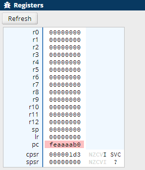
The register is a small physical storage location for the CPU that temporarily holds the data during CPU operations. The register is the fastest form of storage within the entire computer, as it accommodates CPU operations that can be very fast and demand data at a rapid pace.
Registers store the bits inside the flip-flop, which are bistable devices. Each flip-flop stores a single bit, either 0 or 1. Flip-flops are made from transistors, and they are set up in a way that allows them to maintain their state until a clock signal changes it.
The registers are synchronized with the CPU clock, and data is loaded into and read from them according to these clock pulses. So, you can say that the registers have the same speed as the CPU core. The registers are part of the processor’s core. They hold the data that the CPU is working on. For example, if the CPU is working on an arithmetic problem, the register would have the operands and results. Registers are built inside the CPUs, and they offer the first interaction with the CPU in the form of temporary memory.
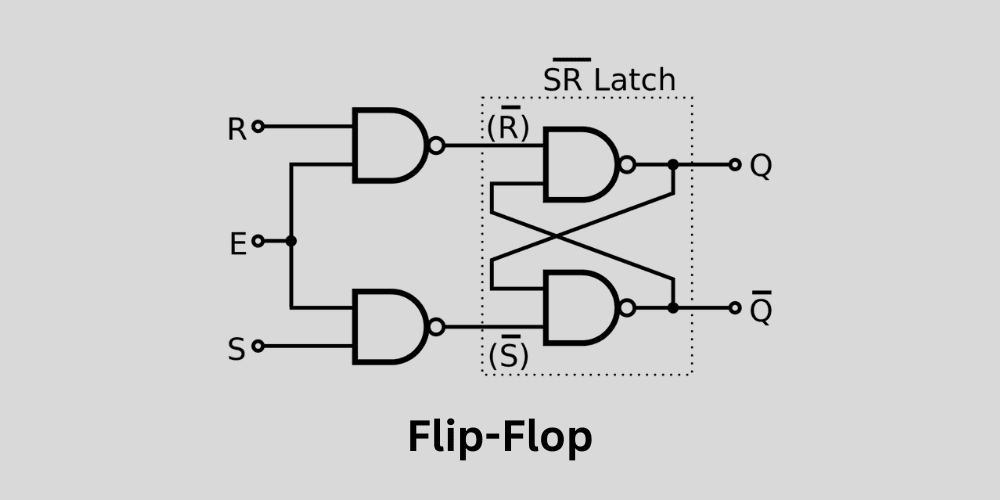
A flip-flop typically has inputs for setting (S), resetting (R), clock (CLK), and sometimes data (D). The flip-flop changes its state only on a specific edge (rising or falling) of the clock signal, which ensures synchronization across the circuit. When the clock edge occurs, the flip-flop captures and stores the input value (0 or 1). This value remains stored until the next clock edge or until a reset/set signal is applied.
Flip-flops utilize logic gates as their working devices, which are constructed using transistors. Neither logic gates nor BJT (Transistors) are storage devices. Flip-flops just remember their state as long as the incoming signals are present. So, the output will remain the same as long as the input is the same. This is the reason flip-flops and hence the registers are temporary memory components. However, they are swift because transistors have pretty impressive switching rates, which are utilized as memory for the CPU. This makes them very suitable for CPUs but very expensive to use elsewhere with higher storage volumes.
2. Cache Memory (L1, L2, L3)
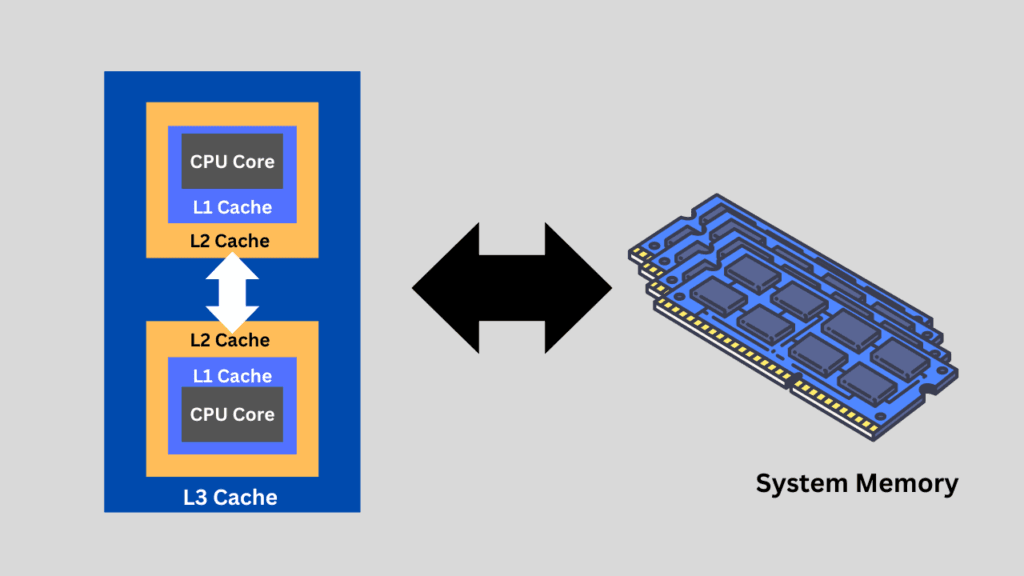
Cache memory comes after the register, and it is built into the CPU just like the registers. However, it typically uses the SRAM, which works almost similarly to flip-flops. The SRAM is composed of flip-flops, but it is slightly slower than the register and faster than the main memory (RAM). Being inside the CPU, cache memory isn’t part of the core but is very close to the CPU. L1 and L2 are generally integrated inside the CPU cores. L3 is located outside the cores, serving multiple cores simultaneously. Cache memory mainly acts as a buffer between the main memory and the CPU. The primary purpose of cache memory is to accelerate frequent data access.
L1, L2, and L3 indicate the speed and the location of the cache. L1 is the nearest to the CPU cores and the fastest with the smallest size. The L3 is the farthest from the CPU, with low speed but high storage capacity.
Inside the cache, the bits are stored in flip-flops and sometimes in DRAM. The process of storage is similar to that of registers, but the cache isn’t as fast as the registers because it does not operate at the same clock speed as the CPU. However, the size of the cache is increased, allowing it to store more data than registers. The cache is more complex in structure. Some cache memories have additional logic for other operations, like cache lookup and tag comparison.
3. Main Memory (RAM)
Main memory, also known as RAM, is the set of RAM chips that serves as a larger storage volume for temporary data storage. This memory is slower than the cache and register memory, but is easily scalable to large storage capacities.
3.1 DRAM
DRAM is the primary type of storage used as the main memory in computers and other devices. It temporarily stores the data and instructions that the CPU needs to access quickly.
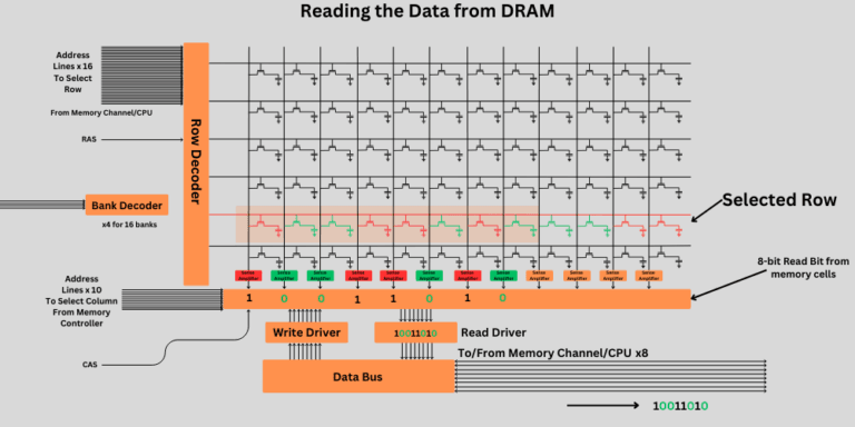
In DRAM, a single memory cell utilizes a capacitor and transistors to store a single bit of data. The capacitor, when charged, represents the bit value “1” and “0” when discharged. The transistor acts as a switch to read from or write to the capacitor. Memory cells are organized in a grid with multiple rows and columns. The word line connected to the row selects the row from which the cell is read or written. The bitline is connected to the transistor and is used to read and write data to and from the cell.

To store a bit, the CPU sends a command to the memory controller with the memory address for the desired data. The address is decoded to specify the row and column and locate the specific cells. To charge the capacitor, a voltage is applied through the transistor. The word line is activated in the correct row, which turns on the transistor, and the voltage is pushed.
When reading the data, the transistor is activated again through the word line, and the sense amplifier checks the charge level in the capacitor. However, after reading the data, the capacitor is discharged, and to retain this bit, a refresh cycle is given. This refresh cycle rewrites the data from the read cells, maintaining data integrity.
4. Permanent Storage
The permanent storage requires no power to hold the data once it is stored in its memory cell. Unlike cache, registers, and RAM, permanent storage drives can retain data even if they are disconnected from our computers. Let’s talk about how they store the bits.
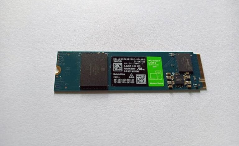
4.1 Solid State Drives
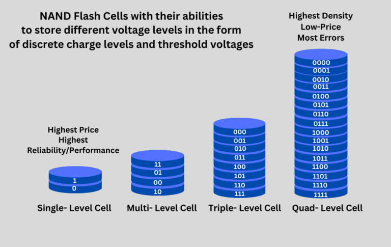
Solid-state drives store data inside NAND Flash memory cells. Each cell is composed of a floating gate transistor or charge trap flash cell that can trap charge within an insulating layer. Impressively, a single cell can store more than one bit of data.
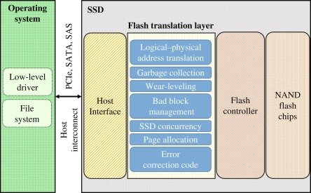
Unlike the RAM, SSDs can’t access individual cells through rows and columns. The smallest readable and writable unit in an SSD is a page, which is around 4KB to 8KB in size. The smallest erasable unit, on the other hand, is called a bloc,k which consists of multiple pages (generally 64 to 256 pages).

The process of storing bits begins in the CPU when it determines that a chunk of data may be required in the future. This command can be triggered by human operations, such as saving a file to a folder. This CPU sends the command via an interface like SATA, PCIe, or NVMe. SSD has a controller that assigns the data to a specific location inside the NAND flash memory cell. However, it cannot simply write the data anywhere. The controller must find a free page that can be written. If it finds a suitable page but it already contains some data, the controller will first rewrite the valid data elsewhere and then write the new data. This is because the controller must distribute the write cycles commonly around the NAND flash to prevent unnecessary wear. This process adds tasks during the writing process, contributing to slower writing speeds.
To read a bit from the SSD, the entire page must be read. The CPU sends a read command, and the controller locates the data. It reads all the data from the page and sends the specified data back to the CPU. The data is read by checking the threshold voltage difference on the floating gate transistor. Different threshold voltages indicate different bit values.
We can take an example of the TLC NAND Flash, which is the most popular in consumer SSDs. These drives can store three bits of data in a single cell. This allows for eight possible different voltage levels to be interpreted as distinct bits. This increases the storage volume but reduces the lifespan and performance of these drives.


So, the bits are stored in the form of different voltage levels inside the NAND Flash cells. The controller inside the SSD is the main component that handles the storage and retrieval of this data. There are many algorithms to ensure data integrity and handle other management tasks such as wear-leveling.
4.2 Hard Drives
Inside the hard drives, the data is stored in the form of varying magnetic particles on the magnetic disk platters. These platters are made up of aluminum or glass and coated with a magnetic material. These platters are divided into nanoscopic tracks and sectors. A track is simply a concentric circle on the platter surface where the data is stored. Sectors further divide these tracks, creating small storage spaces (typically 4 KB in each sector). A sector is the smallest addressable unit in a hard drive.

The coating on these disks can be programmed magnetically in different directions to represent bits of data. So, you can say the bits are stored in the form of changing magnetic orientations of tiny regions. There are two orientations of magnets i.e. north and south. Each could be used to store a bit 0 or 1. Hard disks employ different encoding schemes to convert these bits into magnetization patterns and vice versa.
For writing bits on the magnetic surface, the write head creates a magnetic field that magnetizes the specific areas on the platter. The HDD controller instructs the head to move to the particular location where the data should be written. The write head then changes the orientation of that specific sector.
For writing the data, the controller places the read head over the specific sector and detects the magnetic orientation. This is achieved through a phenomenon known as magnetoresistance. These magnetic variations are converted into electrical signals, which are then converted into binary data. So, the bits are actually stored in the form of magnetic orientations.
5. Optical Storage Drives (CDs, DVDs, etc)
In optical storage devices, the bits are represented in the form of nanoscopic pits and land on the disc surface. There is a laser that reads the difference between the reflectivity on these discs and interprets it as 0s and 1s.
The data is stored on and accessed from a single spiral track on the CDs. In DVDs, the bits are stored in multiple layers.
Generally, the pits or depressions on the disc surface are considered the binary value of ‘1’. The lands or the flat areas are considered binary ‘0’.
For reading, the data a thin laser light is thrown to the specific area of the disc, and light is then captured by a photodetector. This detected signal is converted into binary form or digital data. There is also an error correction program that ensures data integrity.
For writing data, there are special disks (CD-R or DVD-R) that come with a recording layer. This recording layer can change its properties with the help of laser light. Generally, the laser beam heats specific regions to create pits, thereby creating 0 and 1 codes. Some rewritable discs come with mechanisms to change these regions to erase and rewrite the data.
6. Flash Drives
Flash drives store data bits just like solid-state drives. Just like SSDs, the bits are stored inside the floating gate transistors. IN 3D NAND SSDs, the charge trap flash is utilized, which is an advanced variant of the floating gate. You can check the SSD section above for details or read this article.
7. Cloud Storage
In cloud storage, bits are stored in data centers or servers that primarily utilize high-end SSDs, HDDs, and other combinations of storage devices. These drives work similarly to the consumer drives but are designed for higher performance and endurance. The data is generally shared across drives for reliability and redundancy. But the underlying storage technology is again SSDs and HDDs.
Conclusion
There are many other places where bits are stored, such as magnetic tapes, external hard drives, floppy disks, and BIOS chips. But, they are either not relevant today or work again on the concept of capacitor or transistor storage. To answer briefly, the bits are stored in the form of an electric current. In temporary storage, this current is flushed as soon as the power is gone, but in permanent storage, the storage mediums are designed to hold the bits using their physical properties.
Thank you so much