Affiliate Disclosure: This post may include affiliate links. If you click and make a purchase, I may earn a small commission at no extra cost to you.
SSDs have now become the most common storage devices for computers. There are various types of SSDs, distinguished by their speed, application, size, and price. But the basics remain the same. All solid-state drives work on similar mechanisms.
The three primary hardware components of any SSD are NAND Flash, the Controller, and DRAM. A software component is also present for communication, optimization, error correction, wear-leveling, and other purposes.
SSDs work by storing data inside floating gate transistors, also known as cells. In most modern SSDs, however, the floating gate is replaced by charge-trap flash cells. There could be Billions of these cells to make a 1TB SSD. These transistors can hold the charge inside their insulating material. Each NAND flash cell can store 1, 2, 3, or 4 bits of data depending on its design. Furthermore, there is a controller on the SSDs that allocates the cell’s location for the incoming data and then creates mapping tables to relocate it when it has to be read.
SSDs utilize NAND Flash cells, along with a faster Interface, such as PCIe, on the motherboard to connect to the PC. The NVMe protocol helps these drives work with thousands of command queues simultaneously. NVMe is also essential to take advantage of the parallelism that the NAND flash inherits.
Anatomy of an SSD

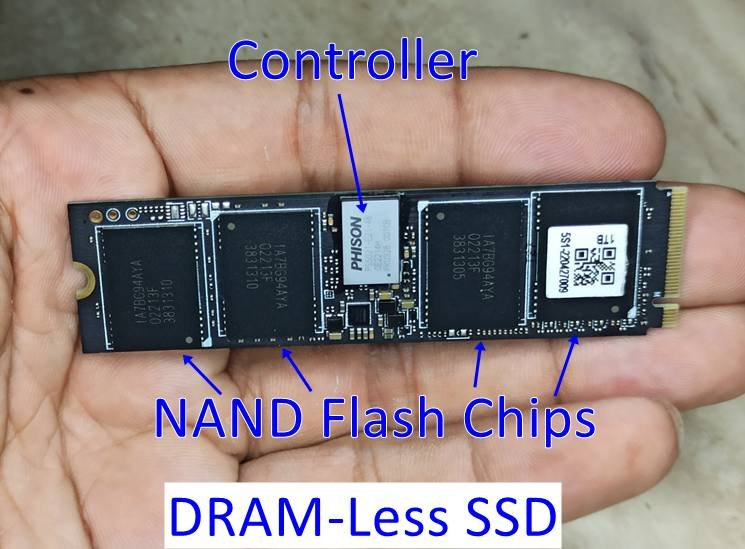
All the components of an SSD are mounted on a PCB (Printed Circuit Board). The connector depends on the drive interface. If it’s a SATA SSD, the port will have a key called B-Key on the left side. In the case of NVMe, the connector will always be located on the right side, designated as M-Key.
The controller establishes the connection with the system through the interface. It communicates with the DRAM and manages data transfer to and from the NAND Flash memory. There are other components like pull-up/down resistors and capacitors for voltage filtering and leveling.
What is NAND Flash in SSDs, and how does it work?
NAND Flash is the central memory location in your SSDs. It is an integrated circuit with many millions or billions of transistors based on the storage capacity. The basic element is the cell, followed by strings, layers, blocks, etc. Let’s start with the cell first, and then proceed further.
1. Cell
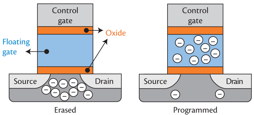
The cell is the most fundamental element inside your SSD. It is composed of a floating-gate transistor, also known as a floating-gate MOSFET. In modern 3D NAND memory technology, a variant of FGMOS is utilized, known as Charge-Trap Flash. It comes with better durability. If you’re unfamiliar with electronics, you may struggle to understand its mechanism. But, in simple words, it is an electronic component that stores the data between two layers of material that don’t conduct electricity. However, the layer that stores the charge is conductive. The two insulating layers create a barrier that prevents the current from dissipating for a very long time.
When millions and billions of these cells are combined, it creates a NAND Flash Memory Cell. Let’s have a look at how the floating gate and charge trap flash memory cell looks.


There can be up to 3 billion or more individual cells in a 1 TB SSD. However, this is the case for the SLC (Single-Level Cell) SSDs. For consumer drives, manufacturers generally utilize a single cell to store three or more bits per cell. This increases the storage capacity in the same space, but also increases wear on the flash. The reasons for increased wear will be discussed later in the article.
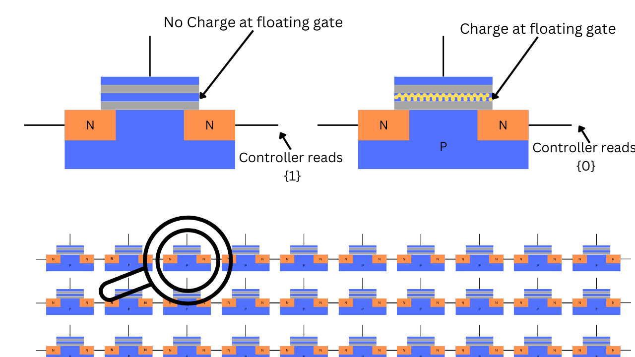
Because the data is stored in the form of bits, the cell enables it to store in the form of an electric charge. You can imagine bit 1 as a charge and bit 0 as no charge.
The concept of bits is just to help humans understand how computers work and program them. There are no 0's and 1's in real. In real, there are just nanoscopic circuits being turned Off and On. When we say one bit whether 0 or 1, we are talking about the presence or the absence of charge somewhere in the circuit.
In SSD cells, the absence of charge in the floating gate transistor mean 1 and if there is a charge, it is considered 0. Writing the data is just pushing this charge inside the gate. For reading, the controller checks whether there is a charge on the floating gate.
It is practically impossible to imagine a cell because its size is pretty small, ranging from 20nm to 10nm. Below is an example image to understand the workings of a floating gate transistor.

Storing terabytes of data with transistors
In 1967, at Bell Labs, two scientists, Dawon Kahng and Simon Min Sze, made the first report on the floating gate MOSFET, although it was invented in 1959 by Mohamed Atalla.
In 1989, Intel was the first company to utilize the floating-gate transistor in its ETANN chips.
It was in the 2000s that the industry transitioned to sub-micron process nodes, producing chips as small as 45nm. In 2010, 3D NAND was introduced, overcoming the limitations of planar scaling. With the help of vertical stacking, the density increased significantly. Now, we are even working with 2nm chips.
Due to the evolution of technology, we can now fabricate billions of these transistors within tiny chips, enabling us to achieve vast volumes of storage. However, at its core, this all comes down to a transistor having the capability to hold a charge within an insulating material. Furthermore, there is circuitry designed to write data in the form of charge and then read it whenever required.

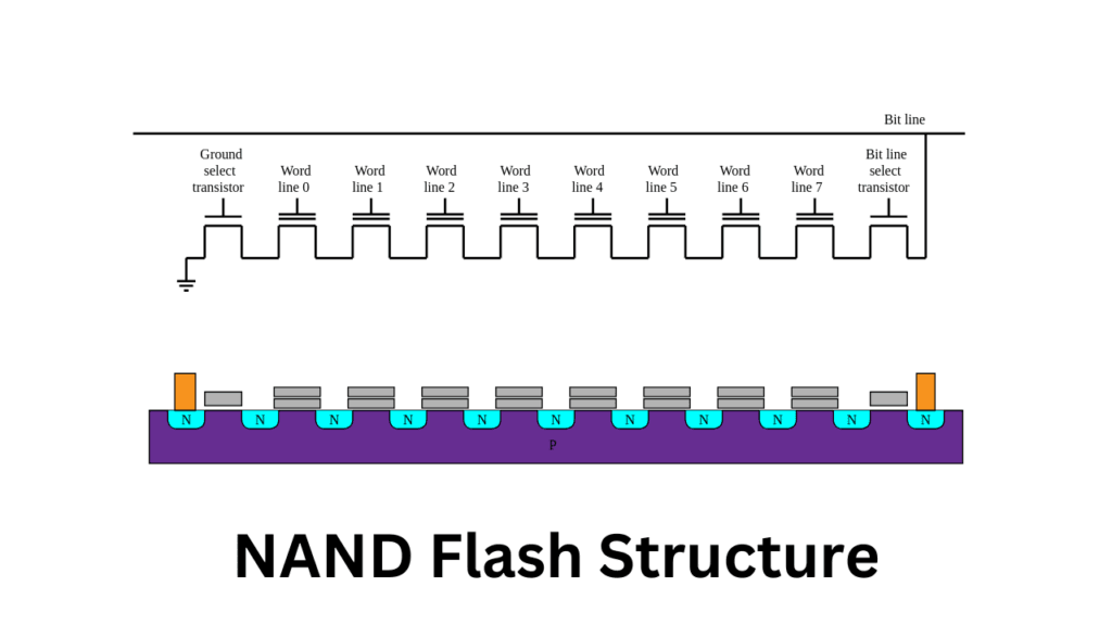
2. Word Line (String)
When we connect multiple Floating gate transistors or cells in a series, it becomes a string or word line. You might have heard that a page is the smallest unit that can be written or read inside the NAND flash, but in reality, a word line is the smallest programmable unit. For the controller to perform its function of reading or writing, a string is switched on with a standard bit line. Then, we can program each cell with the help of a word line.
Typically, there are 16 to 128 cells per string, depending on the type of NAND. In each string, each cell’s ground is connected to the source select transistor. The drain select transistor is connected to the bitline.
The cells inside a page also share the standard word line. But, because the controller properly times the switching, we end up having individual control over each specific cell.
Storing the data in a cell
Now, we have connected multiple cells in a row with the bit line connected to the drains of each. The word line is connected to the gate.
To store the data (program a cell), we apply a voltage to the word line. The charge is stored inside two insulating layers around the floating gate.
Imagine a TLC SSD. We want to store this series of binary bits: “0 1 1 0 1 0 1 0 1 1 1 0 1 0 1”. We will set the voltage levels to those equivalent to “011”, “010”, “101”, “110”, and “101”.
We just stored 15 bits inside just five cells. If we had to do the same thing in an SLC SSD, it would have consumed 15 cells. In QLC, we can store this series in just four cells.
3. Page
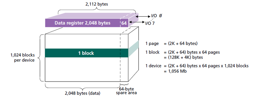
After the Cell, the following fundamental element of NAND Flash is the page. It is a group of cells combined to create a size of 2KB to 16KB. By the way, a page is the smallest unit of NAND flash that can be written. So, if the page size is 2 KB, it’ll have to use at least 2 KB of space, even if the data is less than 2 KB.
The page has a larger size, and the NAND flash doesn’t work on individual cells to conserve energy and simplify operations. This also facilitates compartmentalization, making it easier for the controller to run algorithms such as wear-leveling and garbage collection.
We can use individual cells to store data as it comes, but this will make the tracking process more challenging and also increase the likelihood of errors.
The erasure and programming of individual cells are prone to errors because they can interfere with other nearby cells. But when we write the whole page, it reduces the overhead.
The cell must be activated by the control line to write or read data from and to the bit line. You can imagine a bit matrix with cells at the center connected to the bit line and control line. To access data from any cell, both the control line and bit line must be active simultaneously. The same goes for writing the data.
So, there are cells connected vertically, forming strings. Then, there are cells connected horizontally called pages. A multiple of these spanning a flat area is called a layer. Then, multiple layers create a block.
The page is present so that the control line and bit line can be synchronized to access a single cell. This facilitates the execution of algorithms and the allocation and retrieval of data.
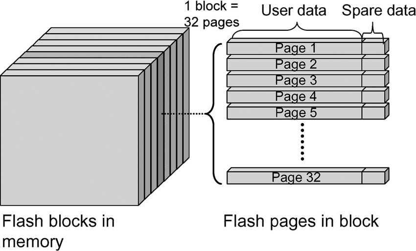
4. Block
A block contains many pages, and they are stacked vertically, as you can see in the image below. A block is generally 64 to 512 KB in size. The erase operations are performed on the block level. So, we can’t erase a specific page from a block. To modify a single page within a block, the entire block is first copied to the cache and then modified there. The whole block is either erased or marked as “free” by TRIM for Garbage collection algorithms. The entire block is generally written to a new location with the updated page.
5. Plane
A plane is a combination of multiple blocks; a single die can have various planes. They are parallelizable. The number of blocks in a single aircraft depends mainly on the type of NAND flash. The number increases as the cells become denser, i.e., fewer planes in SLC compared to more in QLC.
6. Die
If a plane is 16 GB and a Die has two planes, it becomes a 32 GB die. In 2D NAND, a die can have from 1 to 4 planes. However, in 3D NAND, the minimum is 2, while eight is common in consumer drives. Enterprise 3D NAND flash can have 16 jets in a single die.
Writing the data in a cell
By default, all the memory cells are set to “1,” i.e., they have no charge stored in their floating gate. Therefore, if we need to write the data, we must store the charge and set it to “0”. Technically, a charged or programmed cell indicates a bit value of “0” and “1” when erased or discharged.
Now, if we want to store a series of multiple zeroes and ones, we use various cells for this purpose. According to the requirement, the controller writes data or leaves the cell unchanged. Each cell is enabled by its gate voltage being turned on, and then a voltage is injected through the process of tunneling.
Reading the data from a cell
Reading the data is similar in terms of mechanism. To determine whether the cell has 0 or 1, the threshold voltage is checked. If the cell is charged, i.e., it has a logic of 0, the threshold voltage becomes higher. Conversely, the threshold voltage decreases when no charge is stored inside the cell.
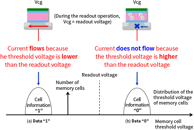
The controller features separate circuitry to monitor these voltage levels and determine the state of each cell. This process is done at a very high pace, generally more than 1 billion times per second, in a 1 GHz controller.
The data is interpreted through the word line, while the bit line is used to enable specific pages within the blocks. There could be up to millions of blocks inside a 1TB NAND Flash chip. The number of pages can be up to 100 million, all within the same size as NAND Flash. When it comes to speed, everything boils down to the clock speed of the controller and the compact design of the NAND Flash chips.
Working with the System
The PCIe NVMe SSDs connect to the CPU directly through the PCIe lanes. This allows the CPU to fetch the data from the drives at a high speed and with a lower latency. Then the CPU can decide to store the data inside the RAM if required. In the case of SATA drives like SATA SSDs and Hard Drives, the data has to go through the chipset, and the CPU has no direct access to it.
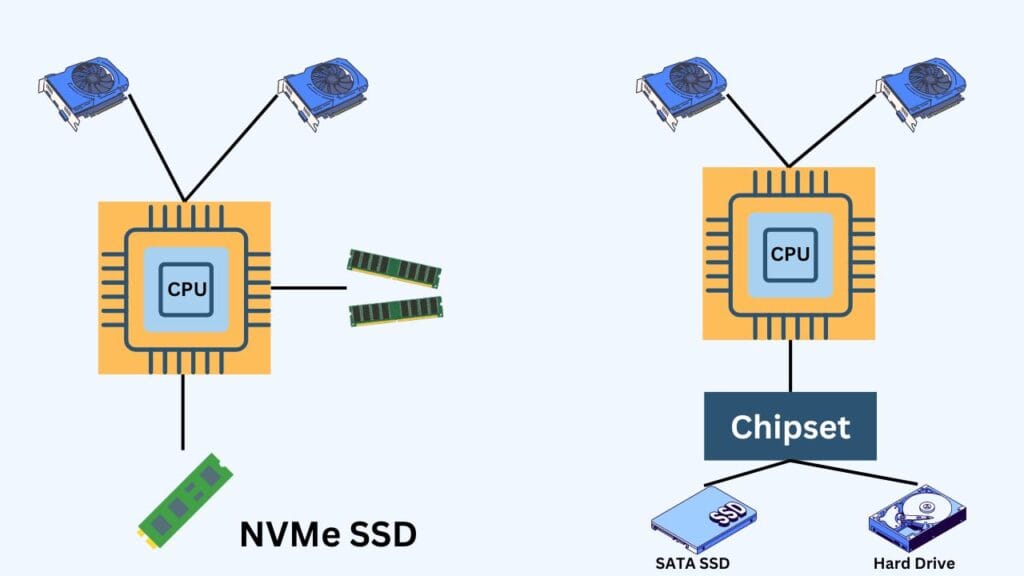
Note: SATA SSDs connect to the CPU in the same way as older hard drives. The path goes through the chipset. This makes them slower than the PCIe NVMe drives.
SSD Controller and its importance
SSDs have their own controllers for interacting with the system and running various algorithms to enhance efficiency and performance. They typically have their own DRAM, which aids in mapping, buffer writing, wear leveling, latency reduction, and other functions.
So, whenever there is an income command from the CPU to store the information or to fetch the data, it goes through the SSD’s controller. The controller on the SSD handles the workload required for data mapping and the algorithm, which otherwise has to be done by the CPU on the motherboard.
The controller runs various software and algorithms for wear leveling, garbage collection, bad block management, TRIM, encryption, caching, interface management, etc.
SSD DRAM and Its Importance
Some SSDs come with dedicated DRAM chips. Because DRAM is much faster than NAND flash, it is used to create temporary mapping tables for the data. It can also act as a write buffer and a storage for metadata. This helps achieve higher read and write speeds by accelerating the conversion of logical addresses to physical addresses. These mapping tables are then stored in the permanent NAND Flash cell. Around 1 to 5% of the total NAND Flash is separated for these tables.
DRAM is also responsible for caching because it offers lower latency and higher bandwidth. It stores the hot data, which is generally demanded by the CPU. However, SSDs can work effectively without DRAM because, with NVMe 1.2 and later versions, SSDs are capable of utilizing the Host Memory buffer and partially using the main memory for storing the FTL. This can’t totally replace the DRAM, but it’s still a good way to utilize some of the system’s RAM space. Also, with the latest advancements, we can achieve hit rates of up to 98% by using as little as 16MB of system RAM with HMB.
SSD Interface and its importance
SSD Interface determines how the SSD connects to the system. The modern high-speed NVMe drives use the PCIe interface, as we discussed earlier. But, there are other interfaces like SATA and in very old systems PATA.
SATA is slower and has a maximum transfer speed of 600 MB/s. However, PCIe drives are much faster. However, the NVMe protocol plays a significant role here, enabling these drives to work efficiently and rapidly. NVMe is a software component that enables higher command queues compared to standard PCIe lanes. When PCIe and NVMe are combined, we allow the systems to utilize the maximum potential of NAND Flash storage technology.
Also, as the PCIe generations are going forward, we are seeing new SSD releases with tremendous read/write speeds i.e. 10 GB/s read speed.