Affiliate Disclosure: This post may include affiliate links. If you click and make a purchase, I may earn a small commission at no extra cost to you.
RAM is your computer’s temporary memory that works along with the CPU. The CPU uses it to store the data from the tasks it is actively working on. Now, the hard drive or SSD serves as your permanent storage, which you can think of as a pantry. It stores everything, but is slow. Imagine your RAM as the countertop. It is small but fast, which is what helps with cooking in real-time. The CPU is the chef, and it needs to grab items from the countertop, such as chops and stirrers.
Let’s take a bird’s-eye view of how RAM works in a computer.
- You open an app.
- The CPU tells the system: “I need this app’s data.”
- The system pulls the app’s code from the storage (SSD/HDD) into RAM so that the CPU can reach it quickly.
- The CPU fetches instructions or data from RAM as needed — a process that can occur billions of times per second.
How fast the CPU gets Access to this data depends mainly on the communication speed and the RAM specifications, like latency and frequency. You might have seen these specifications when purchasing a new RAM.
Ok, so where does the DDR happen?
DDR, or Double Data Rate, refers to the rate at which RAM can send data to the CPU. Inside the computer, there is a memory bus that acts as a path between the RAM and CPU. Computers work with digital signals, meaning they use pulses of electric current to create, transmit, and process data. DDR is the strategy for transferring more data efficiently using the same signal.
In earlier times, before the advent of DDR (Double Data Rate), SDR (Single Data Rate) mechanisms were used for data transmission in computer memory. But with DDR and its new versions, the speed of transmission between the CPU and RAM has increased. So, it is only about the transmission efficiency and nothing else.
Basics of Data Transfer in RAM
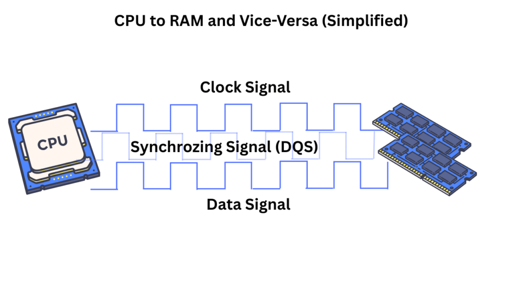
We have already discussed the fact that the CPU stores its most important data temporarily for the tasks it is currently working on. Although they are both placed very near to each other, there is still a path to cover. All the communication between the RAM and CPU happens through the memory bus. The clock signal controls the timing. Data moves along the bus in sync with this clock.
You can call this clock the rhythm that drives the data. Imagine one clock like one beat of a metronome. During each clock cycle, specific operations occur, such as sending or receiving a chunk of data. The speed of this clock (measured in MHz or GHz) determines how fast data can move between RAM and CPU.
RAM doesn’t send data one bit at a time; it transfers data in chunks called words or bursts. For example, a RAM module might transfer 64 bits (8 bytes) at a time. The bus width (number of data lines) and burst length determine the number of bits transferred each cycle.
More about the Clock Cycle
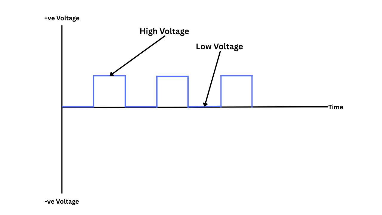
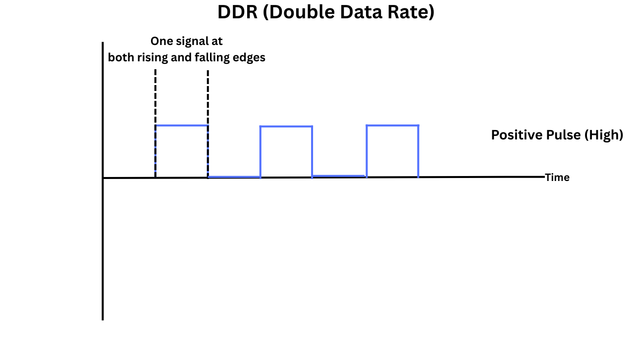
Before proceeding, it is essential to thoroughly discuss and understand the clock signals. The frequency of this clock signal is already set. If you examine image below, you will notice a gap between each rising and falling edge cycle. This is called the frequency, which determines the change and how fast the clock will change. Now, we have set the clock, and we have to use it to transmit the data.
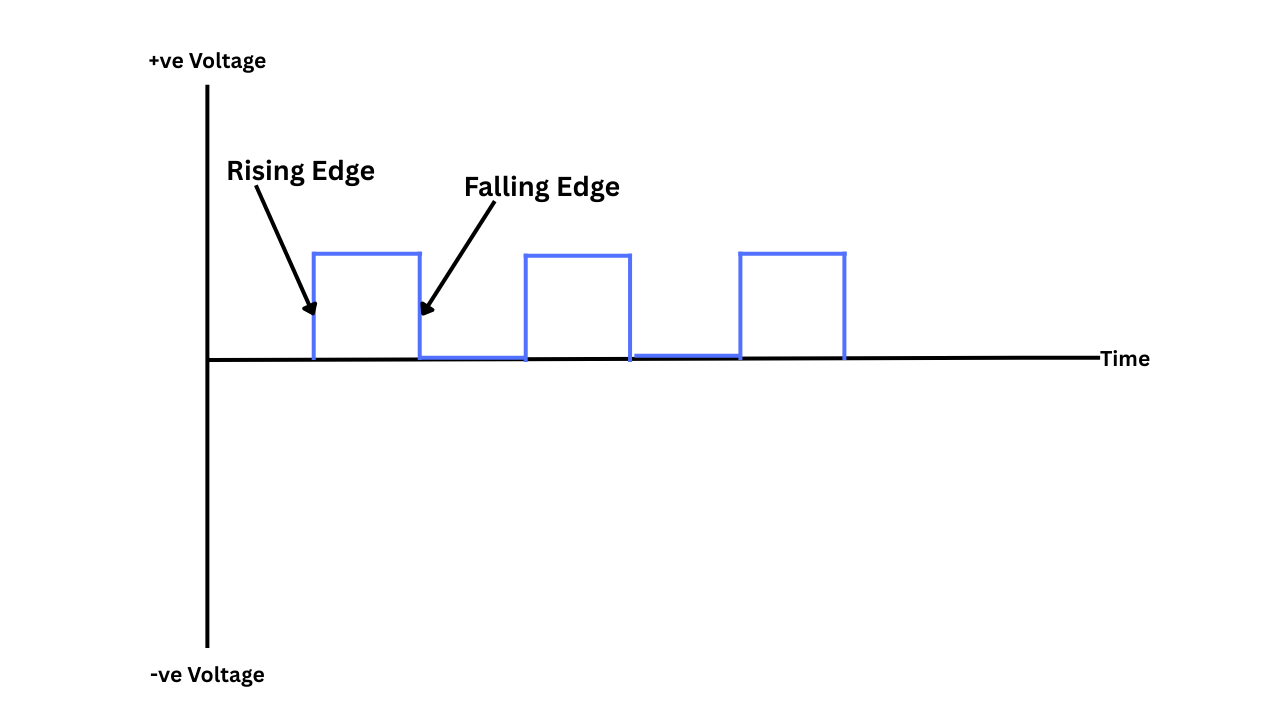
If you examine a clock cycle closely, it has two edges: a rising edge and a falling edge. We use a graph to understand this digital wave, which essentially represents the change in voltage over time. When the voltage increases, it is referred to as the rising edge, and when it decreases, it is referred to as the falling edge. Now, whatever we have to do, we have only this digital clock pulse to work with.
Hertz (Hz) is a unit of frequency used to measure the number of occurrences per second. For RAM clocks, it refers to the number of clock cycles that occur per second. RAM specifications generally say MHz (MegaHertz), which means 1 million clock cycles per second. If your RAM is clocked at 133 MHz, it means it has 133 million clock cycles per second.
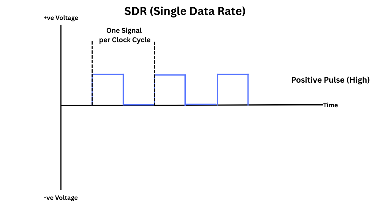
SDR RAM sends data once per clock cycle — typically on the rising edge (when the clock signal goes from low to high).
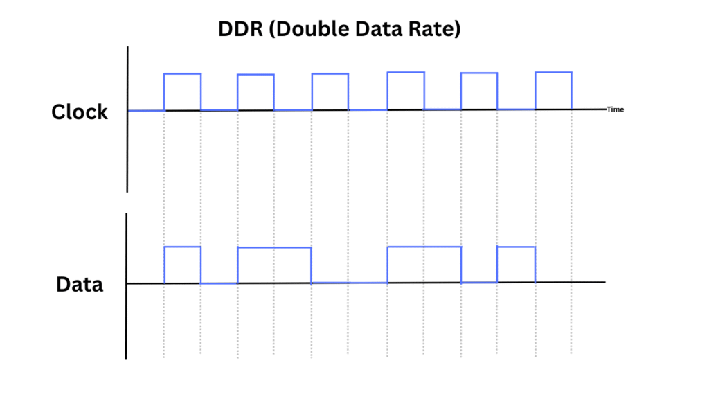
DDR RAM sends data twice per clock cycle — once on the rising edge and once on the falling edge (high to low).
The CPU doesn’t necessarily communicate with the RAM every time data is moved. Instead, a memory controller takes all the memory requests from the caches, queues them, schedules them, and sends them to main memory.
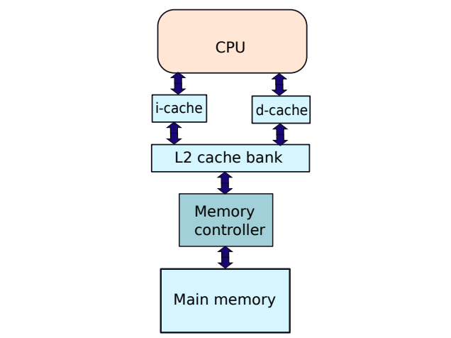
The memory controller is responsible for several critical memory tasks, including address decoding, command sequencing, timing control, and memory refreshing. I have discussed it further in our DRAM article. But here is a simple explanation of how they work together.
Let’s walk through a simplified flow of how they interact. For example, ifCPU wants to read data from DDR4.
- CPU issues a read request for a specific memory address.
- Memory controller receives the request and translates it into DDR commands:
- ACTIVATE (open the row)
- READ (read a specific column)
- Memory controller sends these commands to the DDR memory via control lines (RAS, CAS, WE, CLK, etc.).
- DDR responds after a fixed latency (e.g., CAS latency = 16 cycles).
- The memory controller reads the incoming data on both edges of the clock signal (DDR).
- The controller forwards the data to the CPU.
What is SDR (Single Data Rate)?
Single Data Rate is an older technology that results in wasted clock cycles when considering today’s scenarios. Because it uses only the rising clock cycle, the falling edge is wasted.
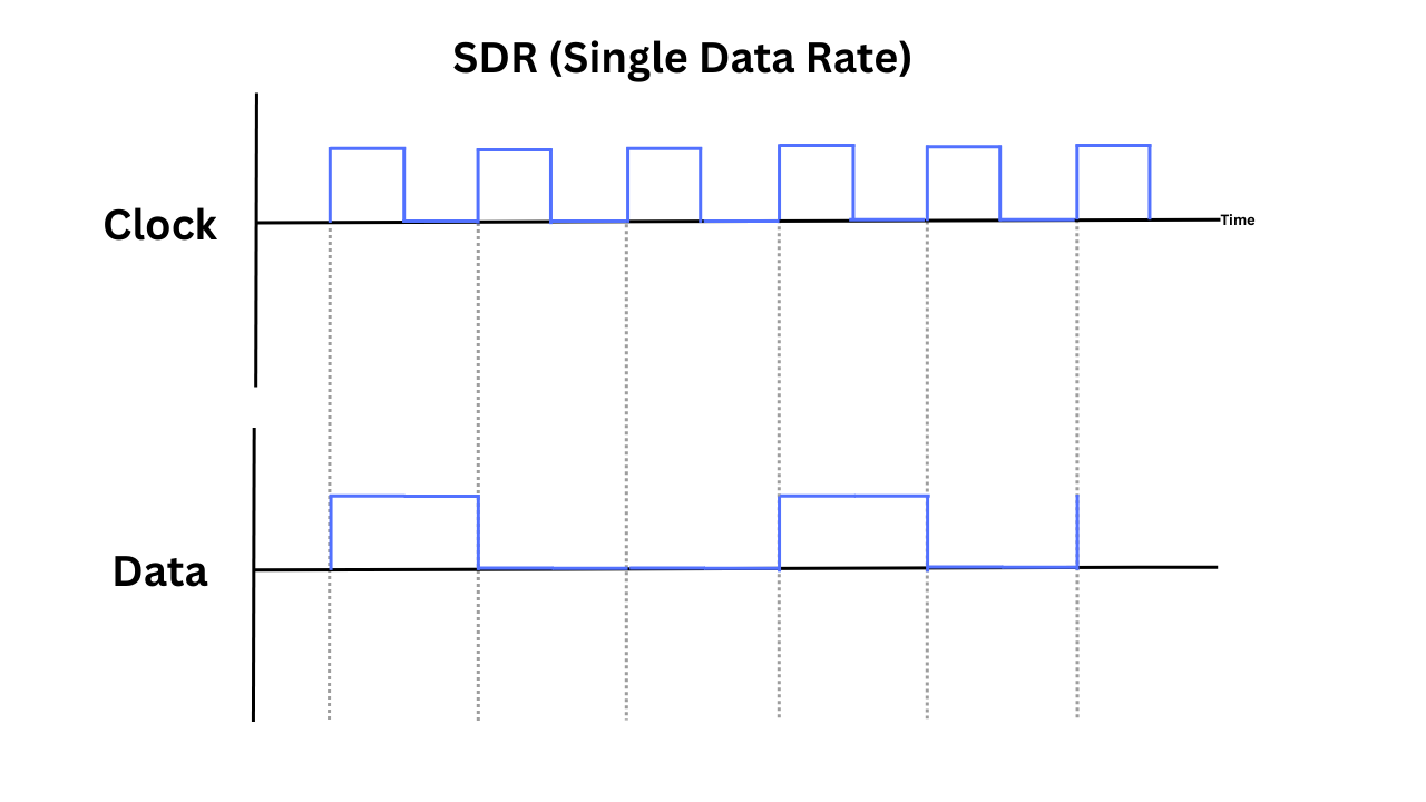
Since SDR is an outdated technology, let’s consider the example of PC133 SDRAM, which operates at a 133 MHz clock and utilizes a 64-bit bus width. Since it sends one word per clock cycle and a word is 64 bits (8 bytes), at 133 million clock cycles, it will have the speed of 1.064 GB/s.
What Does DDR Actually Mean?
At its core, DDR is a technology that transfers data between the RAM and the memory controller (typically located in the CPU) twice per clock cycle, rather than once. It allows higher data throughput without pushing the clock frequency higher.
We discussed the clock signals a little earlier. They swing between two states, i.e., high and low. Each complete cycle includes two transitions:
- From high back to low (called the falling edge)
- From low to high (called the rising edge)
A Generational March: From DDR1 to DDR5
DDR or DDR1
This is the first version of Double Data Rate, where the data transfer rate is doubled compared to SDR. As we already discussed, it is done by utilizing both the rising and falling edges of the clock pulse. But another advantage of the DDR is that it has synchronous operation. It means the memory is timed with the system’s clock, which helps with predictable performance.
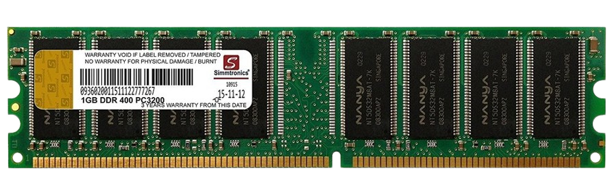
DDR1 modules are typically 64-bit wide, but it is now considered obsolete. In a DDR1 memory module, if the memory clock is 100 MHz, because of the double data rate, the effective data rate is 200 MT/s (megatransfers per second). DDR1 utilizes a two-bit prefetch buffer, allowing it to transfer 2 bits per core clock to the bus.
| Feature | DDR1 |
|---|---|
| Introduced | Around 2000 |
| Data Rate | 200 – 400 MT/s |
| Voltage | 2.5V |
| DIMM Pins | 184 |
| Common Sizes | 128MB to 1GB per module |
| Used In | Older desktops and laptops |
DDR2
It is the second generation of DDR SDRAM, which offers double the speed of DDR1. The basic principle is the same here as well, utilizing both the rising and falling edges of the clock cycle. However, a significant improvement in the internal design is that it uses a 4-bit prefetch buffer, which can transfer 4 bits of data per internal memory cycle. The internal memory core runs at half the frequency of the I/O bus. The DDR2 is less power-hungry than DDR1, requiring just 1.8 Volts.
DDR2 also utilizes on-die termination and additive latency to help stabilize the signals and enhance speed. So, there isn’t a single thing that doubles the performance, but a combination of things. The most important being the architectural change, bigger prefetch, and lower power consumption.
All in all, DDR2 doubled the speed of DDR1, not by making the core faster, but by making data transfer more efficient. This was achieved by utilizing a 4-bit prefetch buffer, allowing more data to be transferred per clock cycle, and increasing the I/O bus frequency while keeping the core speed manageable.
| Feature | DDR2 |
|---|---|
| Introduced | Around 2003 |
| Data Rate | 400 – 1066 MT/s |
| Voltage | 1.8V |
| DIMM Pins | 240 |
| Common Sizes | 256MB to 2GB per module |
| Used In | Mid-2000s desktops, laptops, servers |
DDR3
DDR3 doubles the data transfer rate from DDR2. The prefetch size is increased to 8 bits compared to DDR2’s 4 bits. This means DDR3 can move 8 bits of data per internal clock cycle, twice as much as DDR2. The internal clock of the DDR3 runs at 1/4th of the I/O bus speed, thanks to the larger prefetch.
The voltage requirements are even lower, i.e., ~1.5V. DDR3 also features a Fly-by command/address architecture, which enhances signal timing by minimizing skew between signals. The bank architecture is much more enhanced in the DDR3, enabling better parallelism and performance in multitasking.
The DDR3 memory utilizes a 64-bit bus and boasts a theoretical bandwidth of up to 17 GB/s. The number of banks is increased to 8 as compared to DDR2’s four banks. On-die termination and fly-by topologies are improved for higher speeds.
| Feature | DDR3 |
|---|---|
| Introduced | Around 2007 |
| Data Rate | 800 – 2133 MT/s |
| Voltage | 1.5V (standard), 1.35V (DDR3L), 1.25V (DDR3U) |
| DIMM Pins | 240 |
| Common Sizes | 1GB to 8GB per module |
| Used In | Late-2000s to mid-2010s desktops, laptops, and servers |
DDR4
With DDR4, the prefetch size is doubled to 16-bit. This allows it to transfer more data per memory core clock, which is crucial for achieving higher speeds without significantly increasing the internal core frequency. Unlike DDR4’s single 64-bit channel per DIMM, DDR5 splits this into two independent 32-bit channels, improving parallelism and efficiency.
DDR5 doubles data rates, improves power efficiency, adds on-die ECC, and enables massive memory scaling — all by redesigning how DIMMs handle power, data access, and internal architecture.
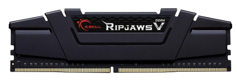
DDR4 also supports high-capacity memory chips, allowing for significantly larger memory capacities. They are more power-efficient and ideal for modern CPUs. Now, since DDR4 is a modern technology, designs have been continually improved, along with the addition of RGB and heatsink options.
| Feature | DDR4 |
|---|---|
| Introduced | Around 2014 |
| Data Rate | 1600 – 3200 MT/s (official JEDEC spec) |
| Voltage | 1.2V (standard), 1.05V (DDR4L) |
| DIMM Pins | 288 (for desktop DIMMs) |
| Common Sizes | 4GB to 32GB per module (up to 64GB for high-end/server) |
| Used In | Mid-2010s to early-2020s desktops, laptops, and servers |
DDR5
Just like earlier versions, DDR5 doubles the data transfer rate of DDR4. This is achieved through a combination of architectural enhancements. The DDR5 speed starts at 4800 MT/s, with a roadmap up to 8400+ MT/s. In DDR4, each DIMM has a single 64-bit channel, while DDR5 is split into two 32-bit channels. Each channel had its own set of rules along with separate control and address lines. This improves efficiency by allowing more simultaneous operations.
The burst length increases to 16, compared to 8 in the DDR4 version. Other features, such as On-Die ECC, enhanced bank structure, and lower power consumption, are available with DDR5.
All in all, DDR5 achieves higher speed mainly through increased data rates and dual 32-bit subchannels, allowing more efficient and parallel data transfer. It also uses a higher burst length to move more data per cycle.
| Feature | DDR5 |
|---|---|
| Introduced | Around 2020 |
| Data Rate | 4800 – 8400+ MT/s (official JEDEC spec, higher in practice) |
| Voltage | 1.1V (standard) |
| DIMM Pins | 288 (same as DDR4, but different key notch and layout) |
| Common Sizes | 8GB to 64GB per module (up to 128GB for high-end/server) |
| Used In | Early 2020s onward in desktops, laptops, and servers |
Developments in DDR6
DDR6 has not been officially launched yet for consumer or enterprise use. The memory industry, led by JEDEC and major manufacturers, is actively developing the standard. According to some sources, the semiconductor industry is accelerating the development of DDR6, with major players such as Samsung, Micron, and SK Hynix having advanced beyond prototypes and entering rigorous validation. These efforts, in collaboration with Intel, AMD, and NVIDIA, aim to deliver initial data transfer rates of 8,800 MT/s, scaling up to 17,600 MT/s—nearly double the current ceiling of DDR5. DDR6 introduces a new 4×24-bit sub‑channel architecture, a departure from DDR5’s 2×32-bit design, to enhance parallel throughput and address signal integrity challenges at ultra-high speeds. To manage physical constraints in DIMM layouts, the industry is adopting the CAMM2 form factor.
DDR Memory Forward and Backward Compatibility
DDR (Double Data Rate) memory generations are not forward or backward compatible with one another, due to significant differences in voltage, signaling, physical layout (pin configuration), and internal architecture. Each DDR generation—DDR1, DDR2, DDR3, DDR4, and DDR5—utilizes a unique key notch position on the memory module, physically preventing incorrect insertion into incompatible motherboard slots.
For example, DDR3 RAM cannot be used in a DDR2 or DDR4 slot, and vice versa. Additionally, the voltage requirements differ: DDR1 uses ~2.5V, DDR2 uses ~1.8V, DDR3 drops to ~1.5V, DDR4 to ~1.2V, and DDR5 goes even lower. This voltage mismatch, along with differing electrical signaling standards (like fly-by architecture or burst lengths), means motherboards and memory controllers must be explicitly designed to support a specific DDR generation.
Even if two generations have similar data rates (e.g., DDR3-1600 vs DDR4-1600), they are incompatible at both the electrical and physical levels.
Additionally, the laptop RAM modules are known as SO-DIMM, and they are not compatible with desktop modules, nor vice versa. They not only have different pin configurations but also different module sizes. So, even if the RAM specifications are the same, you can never use SO-DIMM and DIMM modules interchangeably.
Thanks for reading!