Affiliate Disclosure: This post may include affiliate links. If you click and make a purchase, I may earn a small commission at no extra cost to you.
Whether it’s sequential or random read/write performance, SSDs have higher read speed than write speed.
But, why is that?
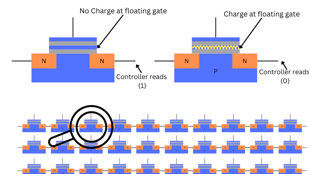
The reason lies in the core technology on which SSDs work. Data is stored bit by bit inside nanoscopic cells called floating gate transistors in the form of electric charge. This is the basic storage unit inside an SSD. But, there are millions and billions of these cells inside a single SSD. They are combined in a way that they are connected to the controller so that the data can be written to and read from through the electric current.
Reading the data is like checking the status of these cells by applying a voltage to the cell. The resulting voltage can tell whether a cell is 0 or 1. However, writing data involves finding the location and generally preparing and emptying space for the incoming data. Along with that, the controller has to create a metadata or mapping table to remember the location and find the data whenever required. Also, the charge must be inserted inside the cells which takes more time as compared to just checking the voltage levels while reading the data.
Over all these, the creation of mapping tables, wear leveling, garbage collection, controller bottlenecks, and extra heat makes things even slower when writing the data.
If all this just went over your head, don’t worry, I am going to explain everything in detail below.
Note: Some images in this article are taken from this research paper from Hung-Wei Tseng
How does an SSD work? (Reading and Writing Data)
Look at the image below of the block diagram of an SSD. This is a simple diagram with fundamental parts of an SSD but there are many other parts in these drives. There are separate software parts as well.
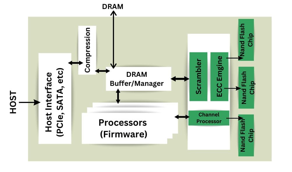
The host (Computer or Server) sends commands to the SSD through the PCIe or SATA interface for either data storage or retrieval. Depending on this incoming command, the controller inside our SSD reacts. If it is a read request, the host will generally send the starting LBA (Logical Block Address) and the amount of data required. This means the command comes with the starting location of that data and the total size needed.
Then the controller locates that location and checks for the data required. The process of transferring back includes compression and some other important elements. But, it is fairly simple as compared to the writing process.
For writing the data, the incoming command comes with the Logical Block Address along with the data that is being written. The incoming data along with the LBA is decoded by the SSD controller first of all. Then The FTL (Flash Transition Layer) maps these logical addresses to physical addresses that are actually present on the NAND Flash.
Before the data is written on the SSD’s NAND Flash, it may be temporarily stored on the DRAM cache inside the SSD in case there is no other write caching involved. In most cases, a faster variant of NAND Flash, called pseudo-SLC is created from TLC or QLC NAND Flash. This step is there to handle and balance the incoming flow of data and forward it to the NAND Flash at a suitable pace.
The structure of NAND Flash (Pages and Blocks)
Using billions of tiny cells inside chips isn’t a simple thing. Not only are there cells, but there are also connections to each of these individual transistors. So, in order to perform parallelism and make the most out of the SSD controllers, the cells are grouped together in bigger units called Pages. A Page normally has a size of 4KB (Around 36000 cells on each page). Each of these cells is connected through shared lines called Word Line, Source Line, and Bit Line on their different points. Page is the smallest unit of NAND Flash that can be written.
After the page, the next unit is blocked. Block is the smallest unit of data that can be erased inside an SSD. Yes, we can’t erase individual cells and even the pages.
Engineers can have control over individual cells but that would be a complete mess to program. But, it is essential not to interfere with the cells. Instead, the whole pages are there to work with with less to no chance of errors.
NAND Flash is special in the sense that it is electrically programmed with such intricacy. However, this comes with many challenges one of which is to decide between reliability and performance.
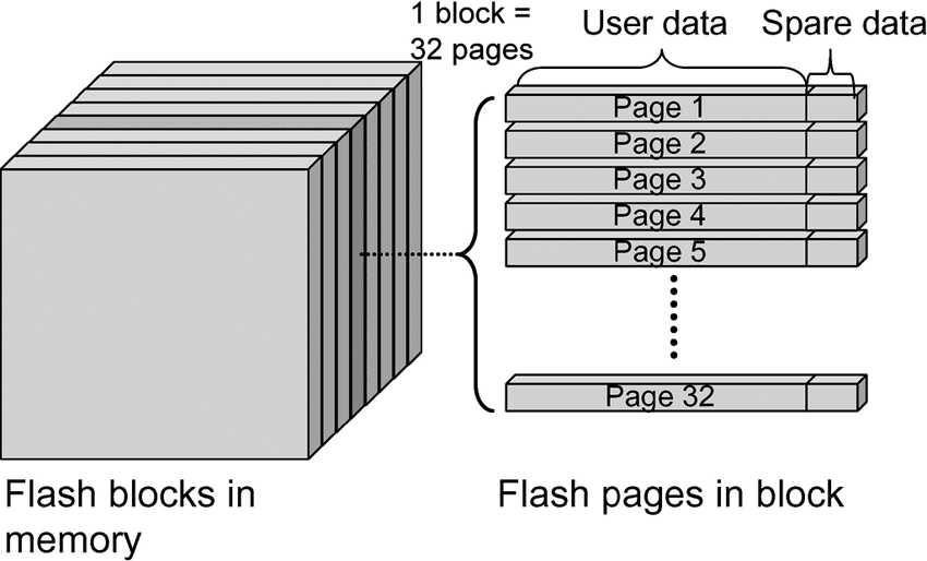
The smallest write-able unit of NAND Flash Memory (Page)
A page is the smallest unit the SSD has to use for writing the data. So, even if the host sends 1KB of data to the store, the controller will activate a whole page because it is connected through the same lines. For writing, specific columns and rows of bit line and word line are activated and the charge gets filled as per the bit structure for that data.
Now, placing the charge inside cells takes a longer time as compared to checking the charge.
If we have sequential data where big chunks of similar data are there, the controller just finds the places and keeps storing the data. Mapping tables are created pretty easily because there aren’t many of these.
For random data where the file size is either small or the data is of mixed kind (small code files, photos, text files, etc), it takes time for the controller to create the mapping tables. Also, this fragmented data has to be stored separately in different locations so that nothing gets mixed up.
The complex process of writing data inside NAND Flash Memory
Inside a page, you can’t directly write the data. The controller has to erase any existing component from not only the page but the entire block with that page. So, if there are other pages inside that block with some important data, they should be moved to a safe location i.e. other pages. Only after that, the controller can write the data on that page. This extra writing load while modification and re-allocation of important data is called write amplification. However, the process of cleaning and reclaiming this invalid space is called garbage collection.

Also, SSDs don’t erase the data immediately after we delete it. It stays there to prevent the drive from unwanted erasures because the Flash cells inside the SSDs degrade after each use. However, there is a logical deletion on the software level that indicates to the system that this block or page is invalid and ready to be erased. This reclaiming of available space is called garbage collection in SSDs.
Three Key reasons for slower data write speed in SSDs
- The first reason is the erase-before-write requirements of the NAND Flash memory. If there is an empty page available for writing, the controller writes it as it is. But, if it has some partial data which is important, it has to erase the entire block and write that important data at another location.
- The second reason is the distribution of wear done by continuous read/write operations to the delicate di-electric material around the floating gate. This di-electric keeps the charge from leaking and can degrade over time. A process called wear-leveling makes sure no same cells are being used for data storage and this obvious damage is separated evenly. This makes the writing process uneven.
- The third reason is the creation of mapping tables which is necessary to find the data when required. This makes the writing process much more complex and adds another layer of storage over the main writing process. There is generally a write cache in SSDs that temporarily stores the incoming data for additional performance but once it is full with the data, the performance again comes back to its original state.
So, overall, this management of the incoming data makes it nearly impossible for the engineers to surpass the write performance in SSDs.
Worse Random write Performance compared to sequential write performance
The sequential write speed has drastically improved with the Gen 5.0 drives but random write is almost similar in both Gen 4.0 and Gen 5.0 drives. This is because the increased bandwidth has nothing to do with how the NAND Flash will behave when it gets a huge management load. This has to do more with the technology itself. Maybe, we get a complete overhaul in the SSD technology and then we figure out ways to achieve much more random write performance.

