Affiliate Disclosure: This post may include affiliate links. If you click and make a purchase, I may earn a small commission at no extra cost to you.
NAND Flash Memory is used in a wide range of applications, including SSDs, flash drives, smartphones, digital cameras, tablets, memory cards, and various consumer electronics. Due to its high-density storage, fast read/write operations, high durability, and low power consumption, NAND Flash is widely preferred for permanent data storage.
This type of memory is the most popular in almost every permanent storage solution. The primary reason is its scalability and lower cost-per-gigabyte compared to other types of Flash memories. However, this scalability comes at a cost of performance and reliability. But that is a topic for another day.
Today, we will conduct a detailed comparison of SLC, MLC, TLC, QLC, and PLC NAND Flash. This topic excites me whenever I write about it. I would like to make it interesting for you here as well.

Working of NAND Flash Memory
In NAND flash memory cells, millions and billions of floating-gate MOSFETs or charge-trap flash cells are combined in a circuit. Because these microscopic cells can hold an electric charge inside them even in the absence of power, it is the basic building block for the NAND Flash. The NAND flash used in modern SSDs is referred to as 3D NAND because it is stacked vertically. But, there are other types as well.
These cells are then combined into larger groups, such as strings, pages, and blocks. The smallest readable and writeable unit becomes the page, and a block becomes the smallest erasable unit.
The most basic NAND flash cell stores one bit of data and can have two possible voltage levels, i.e., high and low. It is called an SL.C memory cell. Manufacturers then customized it to store multiple bits per cell and have different voltage levels, thus increasing storage space while maintaining the same size as a NAND chip and reducing the price.
SLC and MLC NAND flash remained a dream for normal consumers because data centers and enterprise customers were the only candidates who could afford these expensive types of Flash. To understand the workings of NAND Flash memory, we must first understand the workings of the charge trap or floating gate transistor. But, before we discuss the floating gate transistor, we must know a little about the normal transistor.
Normal Transistor (As a switch)
A Normal Transistor has two main applications in electronic circuits: switching and amplification. Imagine having a pipe that carries the water from one end to the other, and a valve controls this flow. Instead of water, electric current is flowing. This is how the transistor’s working can be understood. This is the symbol of a standard NPN transistor. There is another type called the PNP transistor. The functioning of both is the same, but the difference is in the potential of the voltages, i.e., negative and positive.
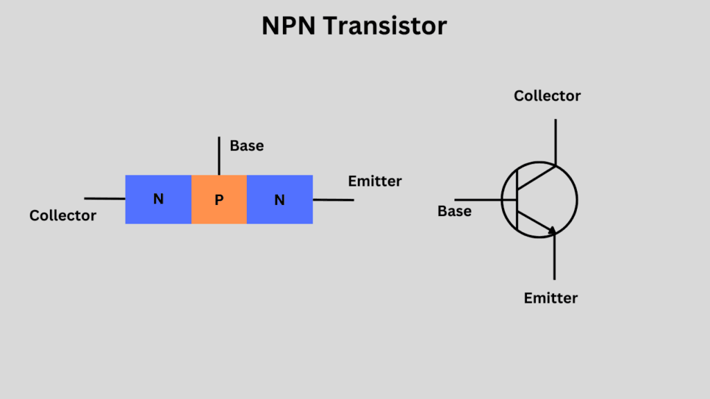
Working on a Transistor
The input current or voltage can be applied at the collector, and some output can be received at the emitter if the gate is turned on with the gate threshold voltage. For the NPN, transistor, the gate voltage will be positive and negative for the PNP transistor. We will not delve too deeply into the formation of transistors, but rather understand the basic working principle. The gate is acting as a switch. If you examine this simplified diagram, the gate voltage functions as a switch to enable the flow of current and also contributes to the primary input voltage at the output.
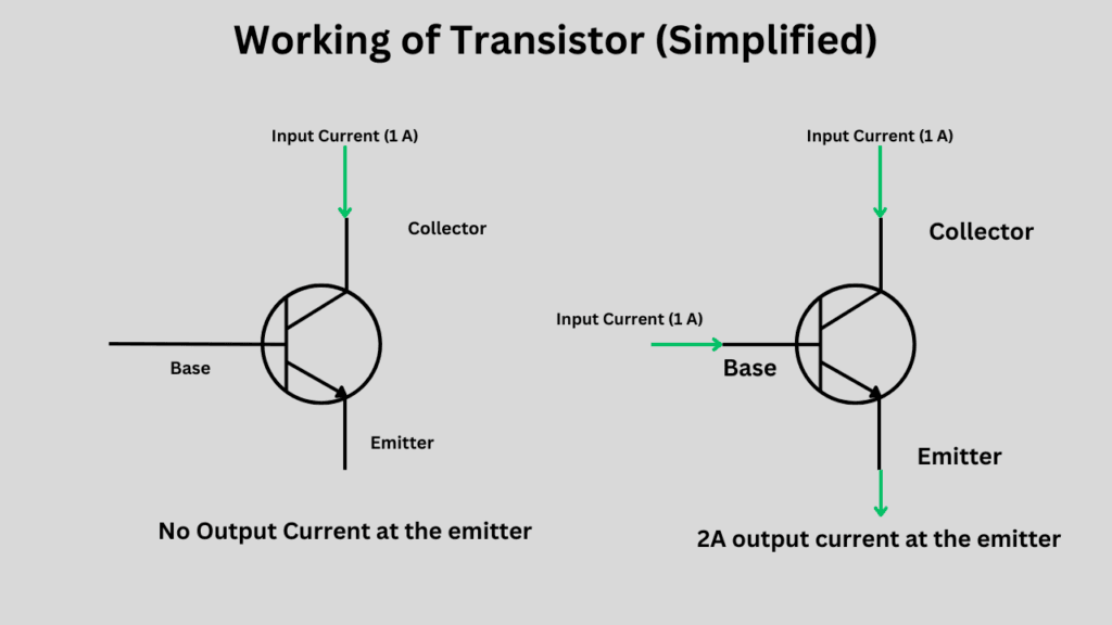
The most important thing about this transistor is that it is switched on at an exceptionally high level of voltage, known as its threshold voltage.
This is all about the normal transistor. It requires power at both the gate and the source to produce an output at the collector. Nothing extra.
Working of a Floating Gate or Charge Trap Flash Cell (NAND Flash cell)
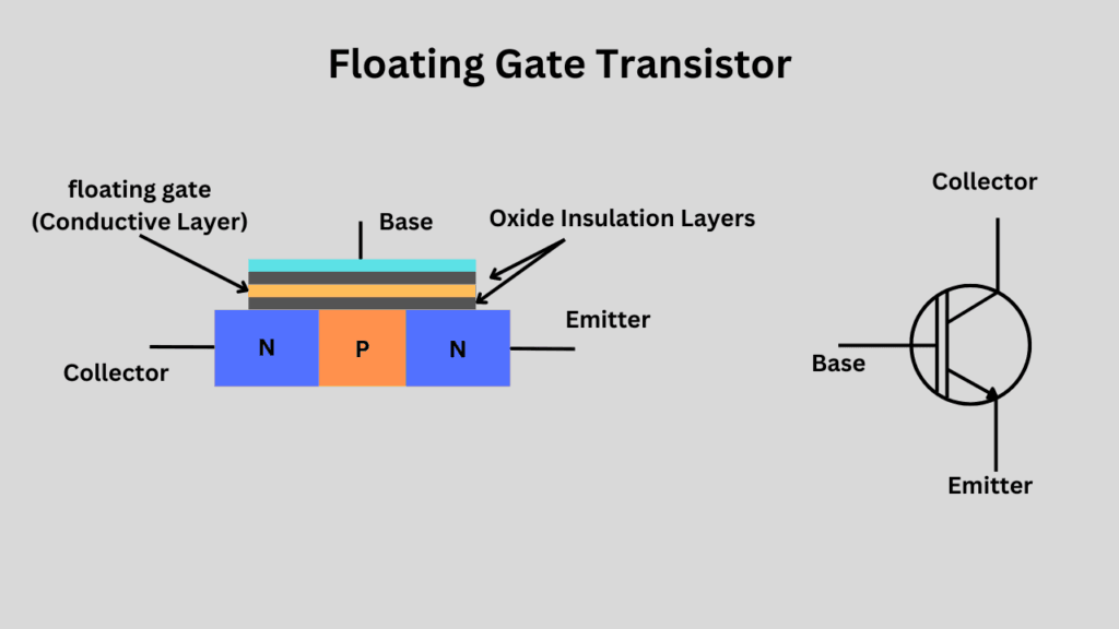

In modern 3D NAND SSDs, floating-gate transistors are almost entirely discontinued. Charge-Trap flash is generally used these days. This cell is similar to a normal transistor but features additional layers, a floating gate in FGMOS, and a charge trap layer in CTF. Additionally, there are two insulating layers surrounding these layers, allowing the charge to be retained in place.
Each cell is connected to three standard lines: the word line (gate), the bit line (drain), and the source line (source). An empty cell without charge resembled the bit value (1) while a cell with charge inside its floating gate resembled (0).
Now, if we want to store this series of bits (1, 0, 1, 1, 0, 1), we must program our cells accordingly. SSDs don’t write data directly to the cells. The controller first clears a block of NAND flash (usually 64KB or 2MB) and then prepares it for writing.
Once a block is cleaned, the data will be written in the appropriate series of cells. When cleared, all cells will be free of any charge and hence set to 1. Therefore, the controller will retain the first cell as it is.
To program the second cell for “0”, it would select the standard word line (gate) for that transistor. A very high voltage will be applied to the control gate. This high voltage will create a powerful electric field across the gate layer. Some electrons from this electric field would jump from the tunnel oxide and reach the floating gate. Now, because the floating gate is insulated, the trapped charge will stay there. After this programming, the controller also checks the threshold voltage to ensure the cell is programmed correctly.
Interpretation of the Stored Bits inside the memory cell
When the controller reads this cell, the same process will be applied, but it will only check the threshold voltage to interpret the presence or absence of charge, i.e., 0 or 1.
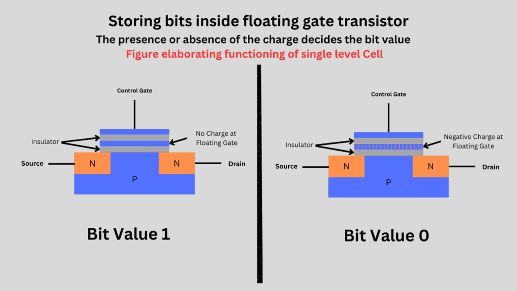
Above, in the normal transistor, we discussed that the gate will have a threshold voltage after which the transistor is turned On. In this case, the threshold voltage will vary depending on whether a charge is stored in the floating gate. For SLC, this presence and absence of voltage will be considered bit value 1 or 0. In the case of multiple bits per cell, this threshold can have various levels to indicate different bit values.
Data Storage in SLC (Single-Level Cell)
Everything we discussed regarding the floating gate transistors and their mechanism pertained to single-level cells. SLC is the simplest type of NAND flash memory, characterized by its simple circuitry and controller programming.
Take one cell from the array of millions of cells in your SLC SSD. If you get into its working and check its floating gate, it will either have a charge or not. That’s it. The condition of this single cell will determine whether the system will read it as 0 or 1.
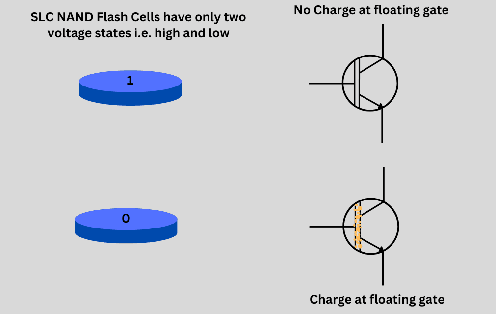
If there is a charge of around 100%, it is considered 0, while a near-empty cell will indicate a bit value of 1.
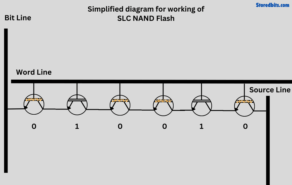
When we combine these cells, we can easily program them to store binary values, which can then be converted into hexadecimal code and other codes that humans and computers both can understand. The exact process will be reversed for storing the data. The codes will be transformed into the bit values and stored in these cells one by one. The SSD or storage controller will keep track of all the data locations in the Flash transition layer.
Data Storage in MLC (Multi-Level Cell)
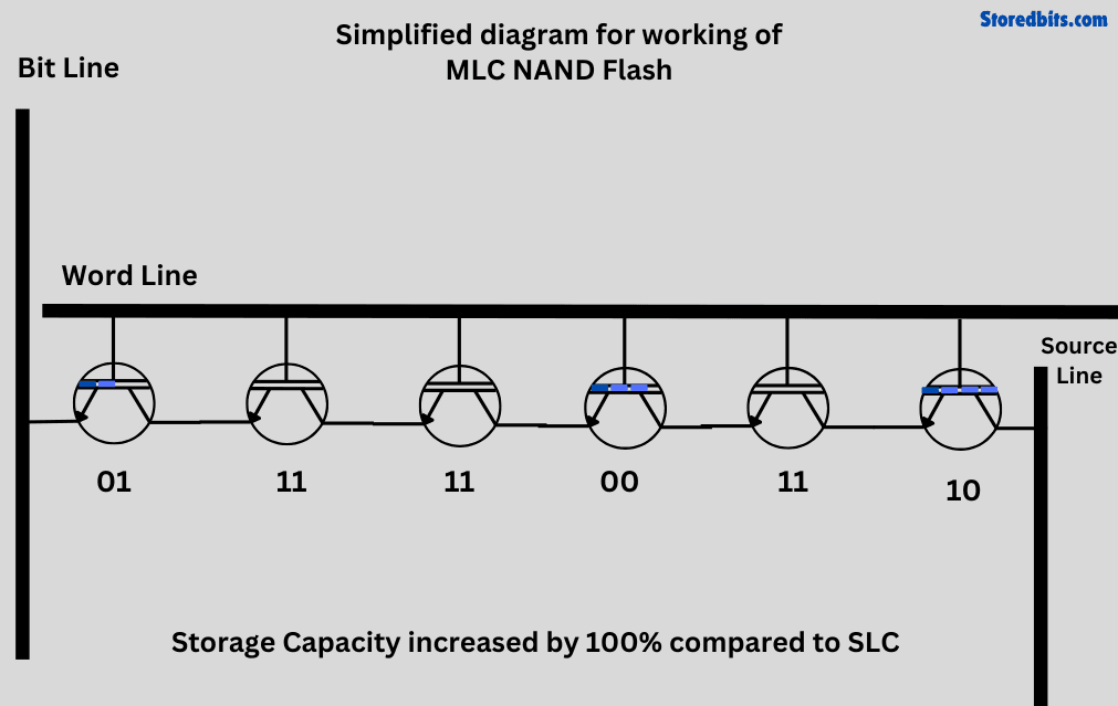
In MLC, a single cell is used to store two binary bits. Since there can be four different unique combinations for two binary bits, a multi-level cell is programmed to store four different levels of voltage.
Generally, a cell fully charged with almost 100% will indicate a bit value of “10”, while an empty cell will indicate a bit value of “11”. Between them lie the “01” and “00” bit values. For storing these values, the controller just pushes the adequate amount of charge into the cell. For reading that cell, it is just about checking the difference in threshold voltage.
These calculations and voltage/current sensors are built inside the controllers, which will perform their jobs as designed. However, the basic idea is to harness the floating gate transistor’s capability to hold different amounts of charge, which can then be sensed back when required.

This all sounds good because we are now capable of storing 11 in a single cell instead of using two different cells and storing 1 and 1 separately. The storage density has been increased by 100%. However, this comes at the cost of reduced performance, lower reliability, and higher latency.
See, if we have to read and write different voltage levels in a single cell, the circuitry will surely become much more complex. The controller will take longer to read and write data because additional time is required to check and create different voltage levels. Also, the data retention time is reduced because the difference between voltage levels decreases. It also results in higher error rates for the same reason. The power consumption will also increase.
NAND Flash cells come with a limited number of program/erase cycles, which is amplified as we start to use single cells for multiple operations. You can read more about P/E cycles here.
Just like SLC, MLC drives have largely been phased out from the consumer market. Mostly, you will find the MLC drives in the enterprise drives and server environments. MLC drives are surely a little expensive but they have the best endurance and performance compared to the upcoming flash types.
Data Storage in TLC (Triple-Level Cell)
The TLC Flash will store 8 different voltage levels in a single cell. This increases the storage density by 50% from MLC and 300% from SLC. Now, a single cell can hold three bits from “000” to “111”. Because the possible unique values between these two numbers have increased to 8, there is a need for finer voltage levels with less room for errors but higher chances of them.
Another difference is that, in TLC, an empty cell denotes 000 while a full cell indicates 111. This is to reduce the risks of overlapping, especially when the cell ages. Now, because the room for taking risks is less, the algorithms must work much more intensively.
So, the TLC becomes much more complex than the MLC. The data retention capability and read/write performance will be reduced because the controller has to perform many more operations for both reading and writing. However, companies can easily put more storage capacities in the same size as NAND flash chips. This opens up room for higher profits but lower endurance and performance.

Now, if we combine multiple TLC cells and use them for storage, we might be able to fit more bits inside fewer cells, but the time taken for calculations and ensuring the accuracy is surely going to be higher. This would result in slower performance, higher latency, increased heat, and a higher likelihood of errors. On the other hand, we get cheaper storage drives and higher storage densities. The drives now have to rely more on the algorithms to prevent wear and errors and to prevent data loss.

TLC is the most common NAND flash in the consumer market. It offers a great balance of performance and price. So, whenever you have to choose between the TLC and QLC, it is better to go for the TLC one.
Data Storage in QLC (Quad Level Cell)
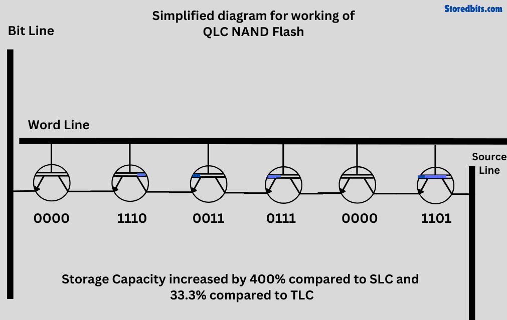
In QLC NAND Flash, a single cell is used to store 4 bits. This increases the density by 33.3% compared to the TLC NAND and 400% compared to the SLC. You can store a series of four bits, so there are now 16 possible voltage levels. The chances of errors and complexity increase a lot more. However, the storage density has increased a lot. This allows the manufacturers to offer very cheap storage drives, but at the cost of performance and reliability.
Because a single cell will be used a lot more, it will have a lot fewer P/E cycles (which will be discussed below). The risks of overlapping voltages increase, along with the demands for much more complex circuitry. The algorithms will have to work with much more power to ensure the data is retained without errors.
For both reading and writing the data, much complex programming is required. Also, the heat generation will be very high even under normal loads.
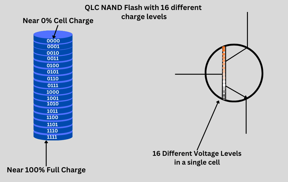
The same cell that was storing just a bit of information in SLC is now storing 4 bits of data in QLC. With just two cells, we can store a byte of data. However, the data retention is reduced,d and the amount of wear is increased. The ECC has to work even harder to get things going without data corruption.
Data Storage in PLC (Penta Level Cell)
The Penta-Level cells are in development but they are going to reach the markets really soon. With this technology, the storage density is going to increase by 500% compared to SLC and 25% as compared to QLC. There will be 32 different voltage levels in a single cell and as a result a lot of errors. To work in the market, the manufacturers will have to employ advanced Error correction codes, wear leveling, temperate control, and many other things.
Detailed Comparison of SLC, MLC, TLC, QLC, and PLC NAND Flash Cells
| Feature | SLC (Single-Level Cell) | MLC (Multi-Level Cell) | TLC (Triple-Level Cell) | QLC (Quad-Level Cell) | PLC (Penta-Level Cell) |
|---|---|---|---|---|---|
| Bits per Cell | 1 | 2 | 3 | 4 | 5 |
| Voltage Levels | 2 | 4 | 8 | 16 | 32 |
| Endurance (P/E Cycles) | ~100,000 | ~3,000 – 10,000 | ~1,000 – 3,000 | ~100 – 1,000 | <100 |
| Raw Write Speed | ~20-40 MB/s | ~10-30 MB/s | ~5-15 MB/s | ~2-10 MB/s | ~1-5 MB/s |
| Raw Read Speed | ~200-500 MB/s | ~150-400 MB/s | ~100-300 MB/s | ~50-200 MB/s | ~20-100 MB/s |
| Error Rate | Lowest | Low | Moderate | Higher | Highest |
| Data Retention | 10+ years | 5 – 10 years | 3 – 5 years | 1 – 3 years | <1 year |
| Power Consumption (Idle) | ~1-2 W | ~2-3 W | ~3-4 W | ~4-5 W | ~5-6 W |
| Power Consumption (Active) | ~2-4 W | ~3-5 W | ~4-6 W | ~5-7 W | ~6-8 W |
| Cost per GB | ~$1-3/GB | ~$0.5-1/GB | ~$0.1-0.5/GB | ~$0.08-0.15/GB | ~$0.05-0.1/GB |
| Typical Use Cases | Industrial, Enterprise SSDs | Enterprise SSDs, Servers | Consumer SSDs, Smartphones | Large-capacity SSDs, Archival Storage | Future high-capacity SSDs, Archival, Read-heavy workloads |
| Temperature Sensitivity | Low (<70°C) | Low (<70°C) | Moderate (<60°C) | High (<55°C) | Very High (<50°C) |
The current situation in consumer storage market
TLC has got over most of the consumer-level SSD market. Even in smartphones and other portable storage devices, you will mostly find the TLC NAND flash. However, whenever you see a storage device with cheap storage, it is surely going to be the QLC.
Most of the time, you will find drives with TLC NAND flash and QLC NAND flash at around the same price points. In those cases, the TLC drives will surely be missing some important features, mostly DRAM and encryption. If it doesn’t have a DRAM, you may have to experience a little poor performance in productivity tasks and the snappiness of the system will be missing.
The QLC drives will generally have lesser TBW as compared to the TLC drives. You may also get more storage capacity in QLC for the same price point but still, if you want your drive to last longer, you should go for the TLC one. If your work includes heavy usage of drives, especially for important data, you should definitely choose the TLC drives.
Conclusion
SLC, MLC, TLC, QLC, and PLC, are just the methods to increase the storage density by using the same physical footprint in solid state storage devices. These devices could be smartphones, flash cards, SSDs, or pen drives.
The basics remain the same. There are billions of floating gate MOSFET employed inside chips and complex controllers are designed to access and write them. There is heavy software running in the background, controlling all the things from interacting with the operating system to keeping track of all the data.
However, these methods for using a single cell for storing multiple bits are now reaching their saturation point because the room for discrete voltage is going less and less. However, Penta-Level Cell NAND flash still excites me a lot. Let’s see how it goes.
Thanks for reading!

![How to Optimize SSD Read/Write Speed? [Expert Guide]](https://storedbits.com/wp-content/uploads/2024/08/cdm-result-768x449.png)
