Affiliate Disclosure: This post may include affiliate links. If you click and make a purchase, I may earn a small commission at no extra cost to you.
In our article about DRAM vs. DRAM-less SSDs, we discussed how DRAM-less SSDs utilize HMB to achieve faster access to the FTL. However, people often confuse DRAM and Pseudo-SLC write caching. In this article, we will clarify that.
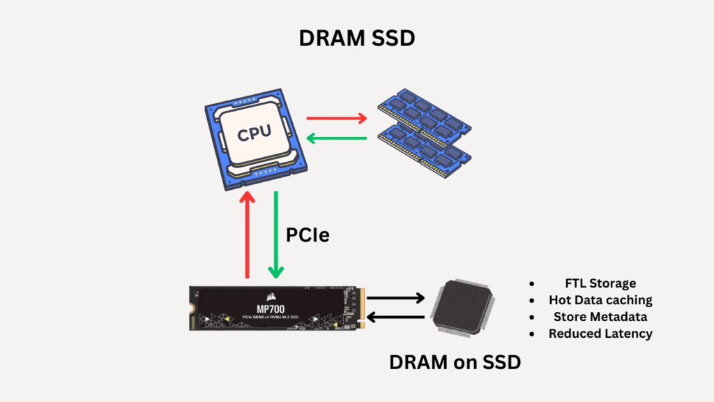
DRAM plays a crucial role in almost everything that happens inside SSDs. It stores the FTL, caches frequently accessed data, stores metadata, and more. If the SSD doesn’t have some sort of write caching, it can also serve as a write cache. However, manufacturers have managed to replicate these features even without DRAM, thanks to HMB.
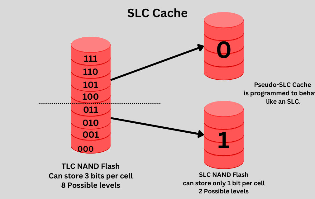
Most modern SSDs use TLC (Triple-Level Cell) or QLC (Quad-Level Cell) NAND flash, which stores 3 or 4 bits per cell, respectively. These are slower to write to and have lower endurance than SLC (Single-Level Cell), which stores only 1 bit per cell. In SLC Caching, SSDs reserve a portion of the NAND to behave like SLC by writing only one bit per cell, instead of three or four.
Without the DRAM, the NVMe 1.2 and later SSDs will use HMB by default. However, there could be SSDs with DRAM and SLC cache, or HMB (no-DRAM) and SLC Cache, or either DRAM or HMB only. However, in most cases, DRAM-less SSDs will have an SLC cache because the size of HMB is generally too small to be used for anything else except caching the FTL. Manufacturers decide to employ these components depending on the price of the drives and other criteria.
What is DRAM in SSDs?
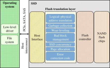
SSDs store data inside NAND flash chips, which include millions and billions of transistors. To keep track of this data, a Flash Transition Layer is used. This layer maps the Logical Block Addresses (LBA) from the operating system to the Physical block locations on the NAND Flash. Because the storage cells are densely packed inside these NAND flash devices, accessing the data can be pretty challenging. Additionally, the operating system requires the storage space to be linear, which doesn’t align with how NAND flash memory works. So, FTL serves as a bridge between the host and NAND flash, ensuring that the operating system receives what it needs and the data locations are correctly registered. Therefore, the controller utilizes the FTL to determine the location of required data and also to monitor the empty spaces.
The primary function of DRAM is to store the FTL and act as a high-speed storage medium for the controller, providing easy access to these mapping tables. Without DRAM, the FTL would be stored in the slower NAND flash or host memory buffer (HMB), resulting in slower performance.
DRAM has another key role as a read/write buffer. Most SSDs these days come with a pseudo-SLC write cache that handles the bursts of incoming (write) data to the drive. However, when it comes to random performance, keeping copies of frequently used data is crucial for improving performance. DRAM does that for you.
DRAM also helps the garbage collection (space reclamation from deleted files) and wear leveling (evenly distributing writes across the NAND) algorithms to work more efficiently. For both these algorithms to function, the FTL needs to be read and updated frequently. With the help of DRAM, this latency is reduced, allowing these programs to run faster.

Understanding the FTL
This topic is important to discuss because it plays a significant role in managing NAND flash memory within SSDs. FTL stands for Flash Transition Layer, and it might sound like a hardware component, but it is a firmware component, or you can say a software component. Its main job is to translate logical block addresses (LBAs) from the host system into physical flash memory locations, because NAND flash doesn’t work like a traditional HDD.
Now, what does that mean?
NAND flash memory has some constraints. The most critical ones are Erase-before-write and Erase in blocks, write in pages. In other words, the data can’t be overwritten in-place. A block must be erased before it can be written. If there is an update to the existing data in a page, the whole block will be rewritten to a new location. You can only write on a page (which is smaller in size) and erase in blocks (bigger). LBA, or Logical Block Address, is how the operating system sees the SSD. To be specific, it views an SSD as a sequential storage space with blocks structured in this manner…
LBA 0 → LBA 1 → LBA 2 → ... → LBA NBut NAND flash doesn’t have an “LBA 1234567” — it has raw pages and blocks scattered across flash chips. So FTL acts like a translator and manager between the host (OS) and the NAND hardware.
Here is an analogy to help you better understand FTL.
- Host says: “Write this data to LBA 1234.”
- FTL says: “I’ll map LBA 1234 to physical page A in block B.”
- It saves that mapping data in its mapping table.
- Later, when the host says “Read from LBA 1234”, FTL finds where it put the data and retrieves it.
- If the same LBA is written again, FTL writes the new data elsewhere (new page).
- Marks the old page invalid.
- Schedules garbage collection to reclaim the old page later.
Let’s say you’re using a 512GB SSD and writing a file. Now, without an FTL:
- The OS would overwrite the same physical block.
- NAND flash would fail quickly due to wear and erase limitations.
However, with FTL:
- FTL writes each new version of the data to a new physical page.
- Keeps the mapping LBA → new page location up to date.
- Eventually cleans up invalidated pages with garbage collection.
How does DRAM work in SSDs?
A DRAM chip is installed on the PCB of the SSD, interacting directly with the controller. Now, when the controller has its own faster memory, it uses it for various tasks that it is programmed to perform.
Let’s discuss the central role first. After your system boots, the controller loads the FTL from the main NAND flash into the DRAM. Now, whenever the controller needs to access the FTL, it will interact directly with the DRAM. If the system is turned off, the SSD will maintain a capacitor-based power supply for the DRAM, ensuring that the FTL data isn’t lost and is stored in the permanent NAND flash memory.
When the wear-leveling or garbage collection algorithms are running, they require metadata to locate free and available blocks of data. When DRAM has this data available, the controller can easily read it at a very low latency.
DRAM is a capacitor-based memory that has a very high bandwidth and low latency. So, it can work great as a buffer. If the SSD isn’t using any kind of write caching, such as pseudo-SLC caching, the DRAM can act as a write buffer to absorb the heavy streams of incoming data and also hold the hot data for frequent read operations.
Whenever a read or write command is sent from the host to the SSD, it first interacts with the controller. If it is a read command, the controller first checks the DRAM for cached data or metadata. If it is not present, it will load the data from the NAND flash to the DRAM. If it is a write command, the controller writes it in the SLC cache (if present) or to the DRAM for a faster write operation.
What is HMB in SSDs?
HMB stands for Host Memory Buffer. The SSDs that don’t come with their own DRAM chips generally use HMB. In this, some space from the system’s RAM is utilized as your SSD controller’s DRAM. However, not all DRAM-Less SSDs are HMB SSDs. Some drives may store the FTL on the NAND Flash or the SRAM that is built inside the controllers. This was common in older, cheap SSDs. The HMB feature was introduced with NVMe 1.2 and its later variants. This opened up new opportunities to manufacture SSDs at a lower cost—also, HMB results in less overall heat on an SSD. However, there are also several drawbacks.
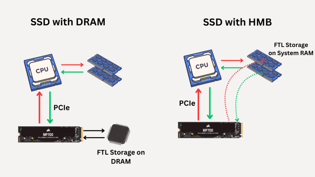
HMB doesn’t fully replicate the DRAM, but it is an innovative solution to enhance SSD performance. HMB stores the FTL but not the entire table. Additionally, it doesn’t generally perform other tasks that the DRAM would typically do. HMB is slower, uses a tiny chunk of your system RAM, and is mostly just for metadata—it can’t buffer writes well or match DRAM’s performance. Therefore, if your SSD has a larger capacity, you may experience performance issues with HMB, especially in random read/write scenarios.
HMB is slower because the data is transmitted through the PCIe interface, which increases its latency. Although RAM is shared through DMA (Direct Memory Access), the latency is still comparatively higher. So, yes, you get benefits in the performance (both random and sequential), but you can’t expect the same results as SSD’s own DRAM.
How does HMB work in SSDs?
HMB is a default feature in the NVMe 1.2 and later drives. So, if your drive doesn’t have DRAM, it will use the host memory buffer by default. Mainly, the operating system decides the size of the allocated HMB. In most modern SSDs, the cache size is typically 64MB, but it can be increased or decreased as needed. The OS may reclaim it if required.
When the system boots up, the SSD controller connects with the NVMe driver on the OS to request the HMB from the RAM. The operating system does this allocation. Once the HMB is allocated, the first thing that the controller does is store the hot mapping entries and cache them in the HMB. The full mapping table is generally kept in the NAND flash for persistent storage.
So, HMB acts as a cache or temporary working area for metadata, not as permanent storage. Therefore, HMB doesn’t replace the NAND-based mapping table; it just acts as a cache and makes access faster. It helps DRAM-less SSDs behave more like DRAM-equipped SSDs,
What is pseudo-SLC caching in SSDs?
Pseudo-SLC caching is an advanced method that converts a portion of the slower TLC/MLC/QLC NAND Flash to SLC NAND Flash. This is done by altering the controller configurations to recognize the multi-level cells as single-level cells. This performance, however, comes with a drawback of lower capacity.
When the data is written to the SSD, it first goes to the pSLC cache, which is very fast and completes the writing tasks quickly. This feature is implemented due to the inherent slower write speed of NAND flash. Once the pSLC cache has absorbed the incoming data, during idle time, the SSD rewrites or compresses that data into TLC or QLC format in the background. So, SLC cache serves as a staging area or to be precise, a write buffer.
Consumer SSDs typically utilize TLC and QLC NAND flash for data storage. More than one bit is stored per cell in these types of memories. These flash memories are dense but slower. Most noticeably, their write speeds are terrible. To boost the write speed (sequential), a pseudo-SLC NAND flash is created.
The manufacturer determines the size of this SLC cache, and when this cache is filled with incoming data, performance falls back to that of the actual NAND flash memory. This caching is used just to enhance the initial write speed. Although this is the perceived write speed, manufacturers will always advertise it as the highest write speed for their drives.
There are two types, i.e., static pSLC cache and dynamic pSLC cache. Static is always available even when the SSD is nearly full. This size if fixed and generally a dedicated space that can not be used for anything else. The dynamic pSLC cache is a flexible portion of NAND which can grow or shrink depending on SSD usage.
How does pseudo-SLC Caching work?
SLC NAND Flash is very expensive and used only in data centers and other enterprise environments. But, for consumer drives, engineers created an innovative solution. SSDs with TLC and QLC flash have very slow write speeds due to the complex circuitry and multiple steps involved in erasing, preparing, storing, and managing the written data. Pseudo-SLC caching is an effective solution to overcome this problem.
Pseudo-SLC caching is most beneficial when writing large files to our drives. SSDs store the data inside tiny NAND flash cells. In SLC (Single-Level Cell), one cell can store only one bit of data, i.e., either “0” or “1”. But, with the advent of Multi-Level Cells, the same cell is now used to store 2 (in MLC), 3 (in TLC), 4 (in QLC), and 5 (in PLC) bits in a single cell.
As the number of bits stored in a single cell increased, performance decreased due to the complexity. With a single bit in a single cell, read/write operations become very fast, but we have to compromise on storage space.

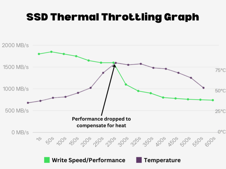
In the graph, you see a sudden drop in the performance that goes even below the performance of the non-SLC write cache graph. This is because once the SLC cache is filled with data, it starts to write the data back to the normal NAND flash, which takes time. Additionally, the controller begins to reprogram those cells to now store more than one bit of data.
In Samsung SSDs, you may have heard about the term “TurboWrite Technology.” This is what they achieve with the help of Pseudo-SLC caching. It is a way to give an artificial boost to the heavy write operations with the help of simpler working of the SLC NAND flash.
Conclusion
DRAM, HMB, and SLC Caching are similar yet distinct technologies used to enhance SSD performance. Any SSD that comes with both DRAM and SLC caching is likely to offer excellent performance in most scenarios. However, HMB is used to replicate the features of DRAM in budget drives. Still, HMB is great for normal to average workloads. But, in most high-end NVMe drives, you will find both DRAM and SLC caching.

