Affiliate Disclosure: This post may include affiliate links. If you click and make a purchase, I may earn a small commission at no extra cost to you.
DRAM (Dynamic Random-Access Memory) is your computer’s main memory, also known as working memory, used to store data temporarily. Whenever the CPU requires data for a task, it retrieves the necessary data from permanent storage, such as an SSD or HDD, and loads it into RAM or DRAM. There are two common types of computer RAMs, i.e., DRAM and SRAM. The RAM sticks that we install in our computers are DRAMs. In this article, I may use either name, but both would mean the same thing.
DRAM is a type of volatile memory that requires constant power to maintain the data stored within it. It requires continuous refreshing, even just to keep the data in its current state. However, it comes with the advantage of high bandwidth and low latency. A DRAM chip can be up to 2000 to 3000 times faster than the fastest SSDs on the market. This speed is required because CPUs need constant access to a temporary storage location, which should also be pretty fast. DRAM, due to its simple structure and faster storage medium, achieves this performance. Faster CPUs require higher frequency RAMs. RAM makes a huge contribution to your system’s overall performance.
DRAM stands for Dynamic Random Access Memory. Random Access Memory (RAM) achieves high performance and low latency by selecting random locations throughout the entire memory for storage and retrieval. Each memory cell is connected to a grid of rows and columns or bit lines and word lines. Additionally, every memory location in RAM can be accessed in the same amount of time, regardless of whether it’s at the beginning or end of the memory space. We will know all of this in the upcoming sections. So, let’s get started.
Note: The main memory used in modern computers is a significantly faster and more refined version of DRAM, known as DDR SDRAM. DDR (Double Data Rate) is a method of increasing memory speed by utilizing the existing bandwidth and hardware.

How does your computer’s memory work?
How does DRAM work?
DRAM is the primary location for temporary data storage for a CPU. If we examine the temporary memory built inside the CPU, specifically cache and registers, DRAM offers higher storage capacity at the expense of speed. The CPU connects to the DRAM through a memory bus that runs through the motherboard. The memory bus connects to the CPU pins on the socket and the DIMM slots for the DRAM.
The data generally goes from the CPU to each DRAM chip in 8 bits at a time, and there are many DRAM chips on a single DIMM (Dual Inline Memory Module). There are multiple memory channels (dual or quad channels) to allow more bandwidth. The DRAM can both read and write data on these DRAM chips concurrently.
The basic storage unit or memory location inside the DRAM is a single memory cell with a transistor anda capacitor. There are millions and billions of these cells inside a single DRAM module.
The memory controller on the CPU keeps note of all the data locations of the written data. Also, to read the data, the memory controller sends the address data to access specific locations. Because each chip can work with 8 bits of data at a time, the controller can read or write 8 bits at a time for each chip. A DDR5 RAM module with a 64-bit data line would generally have 8 memory chips with 8-bit data lines. To reach the specific 8 memory cells for reading or writing the data, various address and control commands are sent to the DRAM by the CPU. Also, some commands are sent back as well. We will come to them later as well.
DRAM works on the capacitor-based memory. Each capacitor holds one bit of information either 0 or 1. Generally, 0 volts in a capacitor represents the bit value of 0. However, a fully charged capacitor (generally between 1 and 2 volts) represents the bit value 1. The amount of stored charge is decided by the manufacturers, specifically the DDR versions. With the increasing generations of DDR, the amount of required charge is decreasing. For example, for DDR5 RAM chips, the capacitor is around 1 to 1.2 volts during its full charge.
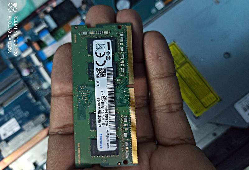
DRAM vs SDRAM
Whenever the CPU needs to read data from the DRAM or write to it, it follows a series of steps synchronized by the DRAM’s clock. So, the CPU’s clock frequency would decide its latency and overall performance. DRAM has its own clock, which isn’t synchronized with the CPU, unlike the SDRAM. This is the reason why DRAM is also called Asynchronous DRAM. The SDRAM (Synchronous DRAM) and DDR SDRAM have taken over the market because of their ability to synchronize with the CPU’s clock. However, SDRAM is a division of DRAM, and both have almost similar working principles, except that SDRAM works much more efficiently with the CPU because of the shared clock. Also, there are some architectural differences between the SDRAM and DRAM
Purpose of RAM in Computers
CPUs are extremely powerful in doing mathematical and logical calculations. But, the limitation is that they can work only with two numbers, i.e., 0 and 1. In reality, there are electrical circuits and components with high (1) and low (0) values doing the calculations. The results of these calculations are again in high and low voltage levels. For example, a circuit can be designed to take two different inputs, either high or low, and provide a specific output, which again could be high or low. But this happens on a large scale. We call these voltage-level bits to create, customize, and understand digital electronic components like CPUs.
For us, the number 1 million is pretty easy to write. We just write 1 with six zeroes after it, just like this 1,000,000. But, in binary, for computers, writing a million would require 20 bits, and a computer would interpret it as 11110100001001000000. The point is that because there are only two numbers available for doing anything or everything, the magnitude of numbers increases pretty fast at a vast scale. The CPU is powerful in performing operations, but due to this increased magnitude, handling data becomes challenging. So, there is always a serious need to store this data temporarily and use it again after a few seconds or microseconds.
RAM comes in handy because of its high performance and low latency, which are achieved by a simple design. It offers a perfect balance of storage capacity and speed. It is placed between the main memory and the CPU’s cache to provide a handy space for the CPU to work effectively.
The purpose of RAM is to hold the data as long as the CPU requires it. If the CPU decides to move that data from the RAM to permanent storage, RAM can be freed from that data. In other words, it can’t be used to store the data permanently. The DRAM would only have the data that the CPU is actively working on. The operating system consumes a significant amount of RAM even when no software is in use. For example, if you open up the Chrome browser, the RAM would have a lot of Chrome data that the CPU needs or will need in the future. All of these things are controlled and optimized by the memory controller, which is built into the CPU.

Key Components of a DRAM Memory Cell
A DRAM memory cell comprises a transistor and a capacitor. Millions and Billions of them are built on silicon chips through very fine manufacturing processes. The size of a memory cell is so small that we can’t see them without specialized equipment. A DRAM made with 20 nm technology, the DRAM memory cell can be as small as 0.0012 µm². At 10 nm or smaller nodes, the DRAM cell sizes continue to shrink, reaching around 0.001 µm² or smaller.
However, to understand, we can draw a memory cell like this, and it’s theoretically the correct representation. It connects to the word line and bit line in rows and columns. We will come to that later.

1. Capacitor
The capacitor is an electronic component that stores electric energy in the form of an electric charge. The two conductive elements are separated from each other to create an internal electric field. This separation could be achieved by a dielectric commonly paper, ceramic, and plastic. A capacitor stores the electric energy but not like a battery. It can store the charge and release it much more quickly. Its major application is in electric filters and power supplies to offer consistent output power even when the input is fluctuating.
In the DRAM memory cells, the capacitor’s capability to store and release the charge quickly is utilized as a very fast storage medium. However, because a charged capacitor will discharge after a very short period, it needs to be constantly refreshed in order to maintain the data in its place. This is the reason capacitors can’t be used in permanent storage devices like SSDs. However, to achieve high read/write performance and lower latency, capacitors are the perfect devices to employ.
2. Transistor
The actual data is stored in the form of charge or no charge inside a capacitor. But, a capacitor isn’t alone in a DRAM memory cell. There is a transistor working as a switch for the capacitor. A transistor separates each capacitor from a huge number of cells inside a cell array.
In electronics, a transistor can be used as a switch or an amplifier. Here, the transistor is used to open up the way for the capacitor. It could either be to read the data from the capacitor or to write the data in it.
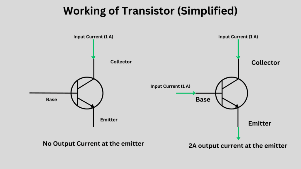
The transistor has three terminals i.e. Collector, Base, and Emitter. The normal path of the current is from the collector to the emitter. But, the flow is controlled by the gate voltage. If we apply a voltage at the base of the gate, the current can go through the transistor to the emitter terminal. You can check the image below for your understanding. There are different types of transistors and various connection techniques but we are sticking just to the basics here.
Basic DRAM Hierarchy (DDR5)
1. A Memory Cell
The fundamental storage unit inside a DRAM is a memory cell. This cell is made up of a capacitor and a transistor and is also called a 1T1C memory cell. The gate of the transistor is connected to the word line, while one terminal (source or drain) is connected to the bit line. The other terminal is connected to the capacitor, with the opposite end of the capacitor grounded or connected to a reference voltage.

Each cell stores one bit of data i.e. either 0 or 1. If a capacitor is full of charge, it represents the bit value 1. If it has no stored charge, it represents a 0 binary value. To activate a capacitor, or to read or write the data, we have to enable the word line first. This is because it is connected to the gate of the transistor. Once the word line is enabled with the specific gate voltage, only then can the bit line be used to read or write the data.
It only takes a few nanoseconds for a memory cell capacitor to fully charge. Now, even if the gate is closed, the capacitor would remain charged for a little while. It starts to lose its charge pretty soon and requires refreshing. A memory cell will be found at an interconnect of a bit line and a word line. However, these lines never connect to each other.
The transistors work as the switch to turn On or Off the capacitor for both read and write operations. However, there isn’t just the transistor. There is a sense amplifier connected to the bit line, which does the job of charging, discharging, and refreshing these memory cells. The size of the transistor is in nanometers. So, the capacitor would keep leaking some current to the bit line even if the transistor is switched off. For, that refreshing is required which we will cover at the end of this article.

2. 2D Memory Cell Array (Subarray)
Millions of these cells are combined inside memory arrays. There could be thousands of word lines and bit lines, depending on the number of memory cells. Here is a representation of a small section of a memory cell array. It is also calleda subarray because it is a division of a bank. We will come to the banks later on.
3. Rows and Columns
The row is known as the word lines and the columns are bit lines. More specifically, the cells that connect to the word line are counted in the row and column for the bit line. As you can see in the image above, each row or word line is connected to a sequence of memory cells. The connection is at the gate or the base terminal of each transistor in a memory cell. If we look at the column or the bit line, they are connected to the source terminal of the transistor in each cell. The column address has the job of selecting the specific bits from the activated row and reading or writing the data to it. We will come to the mechanisms later on.
Each cell is connected at a different intersection of a word line and a bit line. But, as we discussed earlier, word lines and bit lines never interconnect with each other, but only with the respective memory cells. To reach an individual cell, the connecting bit line and the word line must be activated at the same time. Each intersection or the memory cell will have its address that the CPU will use for reading and writing. However, because the DRAM chips are divided into numerous subdivisions, such as banks, bank groups, rows, and columns, locating them using the correct circuitry isn’t particularly difficult.
4. Banks and Bank Groups
Banks are the broad divisions of a DRAM memory chip. In DDR5 DRAM, there are generally 8 Bank groups inside each RAM chip. In each bank group, there are 4 banks ,which becomes a total of 32 banks. Each bank is then divided into rows and columns of individual cells. However, the number of banks and bank groups may vary depending on specific RAM types.
A bank consists of multiple subarrays. This allows for easy and efficient access to specific parts of memory. Banks allow the DRAM chips to perform parallel operations because each of the banks can be accessed separately.
The number of rows and columns in each bank varies according to the speed, size, and manufacturer’s preferences. However, there are DRAM banks with up to ~65000 rows and ~8000 columns. It simply means there could be billions of memory cells in a single bank.

5. Ranks
Each rank in a DIMM chip is a collection of chips that share a common data bus and can be addressed separately. In standard DDDR5 DRAM chips, there are 1 or 2 ranks. In high-capacitor modules, the number of ranks could be higher.
6. DRAM Chip
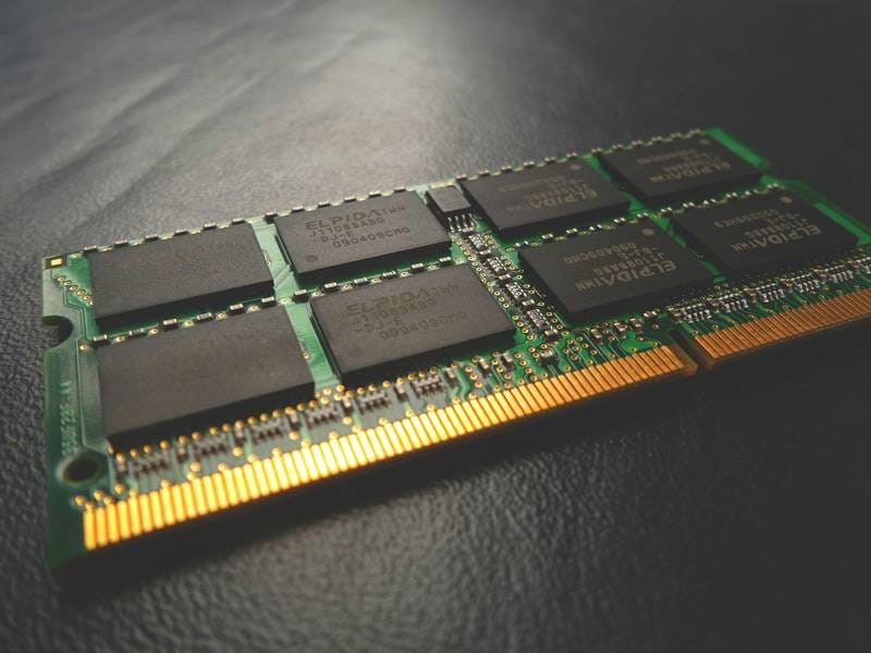
A typical DDR5 module, such as an 8 GB, 16 GB, or 32 GB DIMM, features 8 or 16 DRAM chips. If the module is single-sided, it typically has eight chips. If it is dual-sided, it can have 16 memory chips. However, this depends mainly on the manufacturer.
How does the CPU interact with the RAM?
The CPU interacts with the DRAM via memory channels connected through the memory bus. The memory channels are the dedicated pathways between the RAM and the CPU. A CPU can support multiple memory channels (e.g., Dual-Channel or Quad-Channel), which means the CPU can communicate with more than one RAM module simultaneously. In server environments (CPUs like Intel Xeon and AMD EPYC), the systems can have hexa-channel or Octa-channel memory support. Memory channels decide the total allowed bandwidth for the computer memory.
In modern computers, the memory controller is built inside the CPU. In older systems, it was found in the chipsets. The memory controller manages the data flow between the CPU and RAM via memory channels. It also serves as a mediator between the Cache memory or the CPU and the physical DRAM chips.
The RAM chips are connected to the DIMM slots on the motherboard. The type of slots and number of pins may vary depending on the DDR version of the memory. The DIMM slots are connected to the memory channels that connect to the CPU socket.
The memory bus is the actual physical set of wires (traces on the motherboard) that carry data, control signals, and addresses between the CPU and RAM. Each memory channel would have its own memory bus (a dual-channel system will have two memory buses). The bus width is usually 64-bits per channel. The interaction is mainly controlled by the memory controller because it keeps track of the data locations, addresses, signals, and many other major DRAM operations.
All types of Memory Signals and Buses
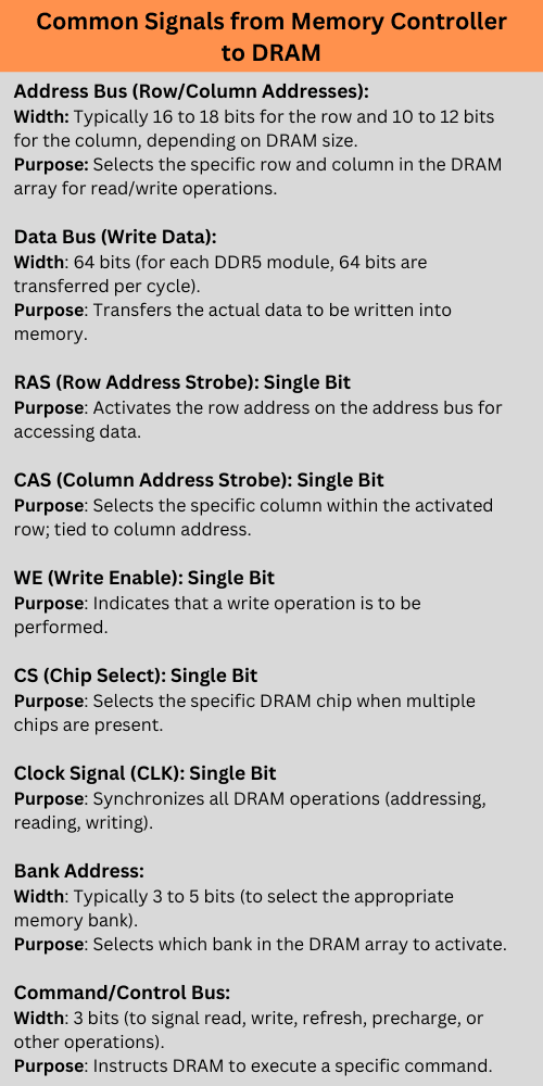
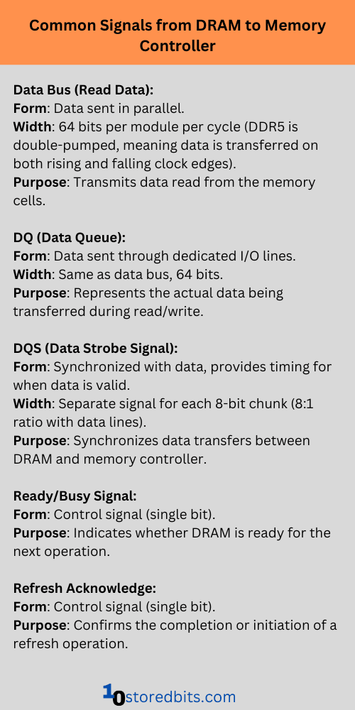
Many types of memory signals go from the CPU to DRAM and vice-versa. These signals do most of the operations of data movements, storage, and retrieval. Again, they are synchronized by the clock pulse of the DRAM.
1. Data Signals (Data Bus)
The data signals are sent through the DQ lines, which are the lines to send and receive data between the CPU and RAM. In DDR4 and DDR5 DRAM, each memory channel has a 64-bit data bus. This means the data is sent in parallel, 64 bits at a time. To a single memory chip, an 8-bit memory bus would be allocated. For example, a 64-bit data will look like this:
11000001 11001110 00110011 11110100 10001010 01111010 10010010 10001100
The data is sent in bursts during the read/write operations. The width of the bus will define the total number of bits being transmitted at a time.
2. Address Signals (Address Bus)
The main purpose of this bus is to define the memory address being accessed. The total capacity of the RAM generally decides the address bus width. The DDR4 RAM can have a 16 to 18-bit wide address bus. To reach the specific memory cell, the memory controller needs to specify the rank, bank, column, and row to which the cell is connected. As an example, the address bus takes the signal in this way to read or write a specific memory cell.
Row: 110001, Column: 101010, Bank: 001, Rank: 00
Again, these signal goes and come in the form of binary code, often in parts
3. Control Signals (Control Bus)
The control bus handles the control signals. These signals decide the type and timing of the specific memory operations. The main control signals are:
3.1 RAS (Row Address Strobe)
The row address strobe is used for the row selection when accessing a memory cell. CPU sends the row signal through the memory controller when it wants to request some data. This strobe signal latches to the row address which tells the DRAM to select a specific row. The RAS signal has the size of one bit either 0 or 1 (High or Low). When the RAS signal is sent to the DRAM, the signal is set to low in order to activate it. The total time taken by the RAS to activate a row plays an important role in memory latency. The faster the RAS, the lower will be the memory latency. However, RAS isn’t alone because CAS plays a much more important role in memory latency.
3.2 CAS (Column Address Strobe)
Just like the RAS, the Column Address Strobe or CAS is the control signal used to select the column to access the specific memory cell. Once, the column is identified, the cell is read or written because it was activated by the RAS. The delay between these two signals is also important in determining the RAM performance (known as tRCD). The CAS signal is always followed by the RAS. However, the data access (read/write operation) is done after a memory cell is accessed by CAS.
When checking for RAM specifications, we often get across a parameter called CAS latency. A lower CAS latency means the DRAM can retrieve data faster. A CAS latency of 30 means the DRAM takes 30 clock cycles to provide the data after the read command is sent. Just like RAS, CAS is also sent in sa ingle binary signal 0 or 1. A low CAS signal “0” indicates that the column address is latched for a read/write operation.
3.3 Write Enable Control Signal
A Write-Enable signal (low or 0) sets the DRAM to the write mode and goes through the control bus. However, when reading the data, the WE signal must be set to 1 or high. The WE signal goes together with the RAS and CAS signals. RAS selects the row, CAS selects the column, and the WE signal determines whether the data will be written to or read from that specific location. The timing parameter tWR is another important parameter deciding your RAM’s performance.
Some other control signals that utilize the Control bus are Chip Select (CS), Clock (CK), Data Mask (DM), Output Enable (OE), Refresh (REF), and Precharge (PRE), etc.
Reading the data from DRAM
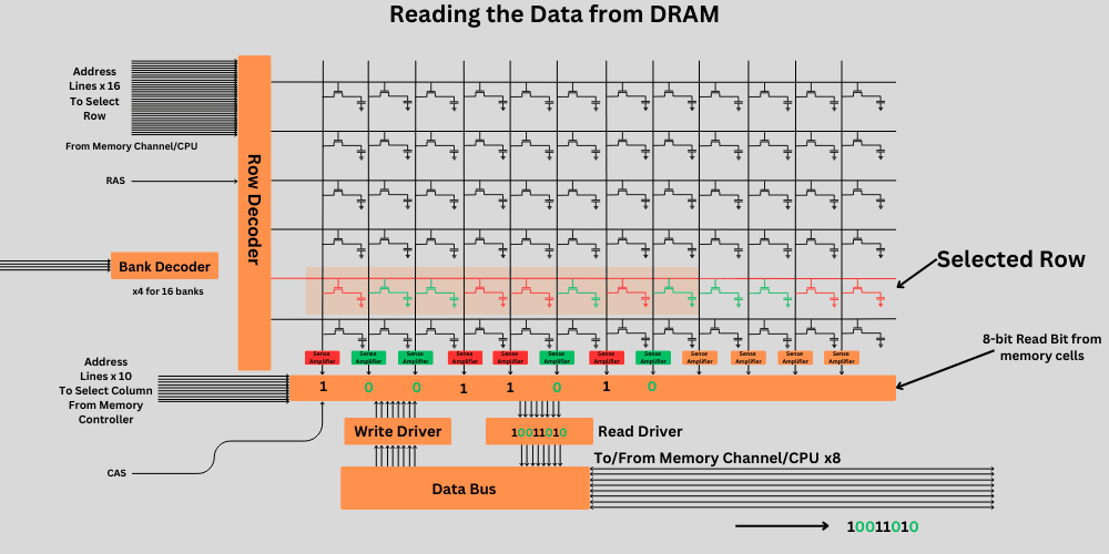
Reading the data is a multi-step process. The memory controller sends the information about the bank address, row address, and column address. First of all, the read command and the address are sent from the CPU to the DRAM. The first five bits select the specific bank from the bank group. Then all the word lines are turned off in the bank to isolate all the capacitors. All the bit lines in the bank are precharged to around half of the full capacitor (0.5V for a 1V full capacitor charge). The capacitor charge voltages may vary, but we are imagining 1 volt as charged and 0 volts as a discharged capacitor.
The 16-bit row address is sent to turn On the specified row. Now, when the memory cells from the row are activated, they start to send some current to the bit line. If an individual capacitor from that row holds full charge, i.e., ~1 volt, some charge would start to flow through the bit line and reach the sense amplifier. The sense amplifier would check the voltage levels and the bit value depending on it. If it is a 0, it would then feed that value to the read driver. The same will happen for each 8 bits.
The column address now connects the 8-bit lines to the 8-bit lines of the read driver. The read driver then sends the data to the 8 data wires that go to the CPU.
Now, because the charge from the capacitor is lost due to this reading, they are refreshed back to their position if the data is necessary. The sense amplifier will set the cell to its original value through the bit line. I have discussed the refreshing mechanism in the upcoming sections of the article.
The sense amplifier is important because of the large number of rows and columns to keep amplifying the stored charge in capacitors. Now, all the bit lines are set to 1 volt or 0 volt, depending on the stored charge of the capacitor in the activated row. This row is called an Open Row.
Writing the data on DRAM
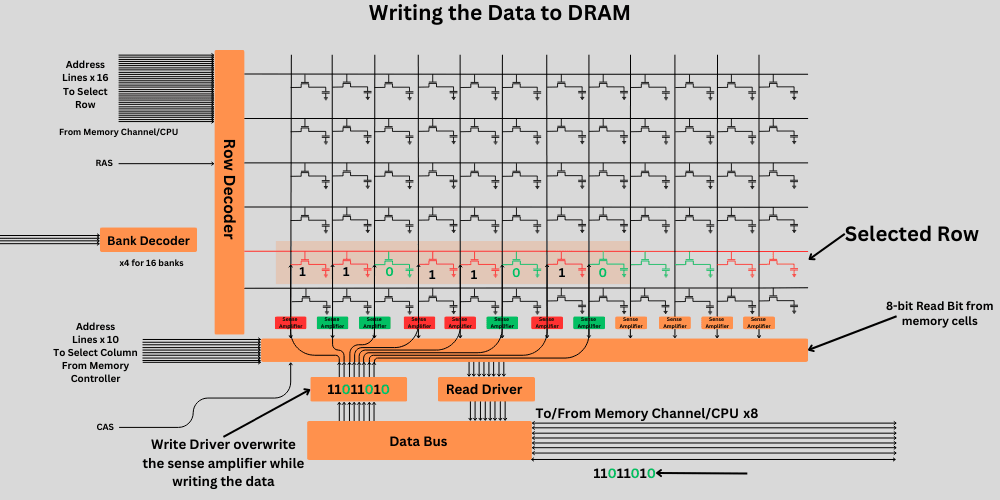
First of all, the CPU places the data to be written on the data bus. For writing the data, the CPU (memory controller) provides the address through the address bus. The address includes the address of specific rows and columns.
Again, depending on the selected bank and row, the capacitors are isolated and bit lines are precharged to 0.5 volts. The sense amplifier sets the bit line to corresponding voltages depending on the status of the capacitor. Along with this, the Write Enable command is sent by the memory controller if the existing data has to be overwritten with the new data.
After the row is activated (via RAS) and the bit lines are precharged, the column address goes to the column multiplexer. The column multiplexer now connects the specific 8-bit lines to the write driver which contains the 8 bits that the CPU had sent for writing. The write drivers are very strong compared to the sense amplifiers. So, they can easily over-write any data that we previously wrote in the memory cell. the specific memory cells for that row and column are targeted. The WE signal is activated (set to 0) to indicate a write operation. The data placed on the data bus is captured and written to the memory cells at the given address.
All these operations are synchronized through a common clock signal. The timing of RAS, CAS, and WE must be aligned properly to ensure accurate data writing.
After the write operation, the row is required to be precharged (deactivated) to prepare the memory for the next access. This is done by deactivating the current row and making it ready for a new row access. DRAM also needs refreshing to retain the data which we will discuss
Row Precharge
Once the data is read or written to the specific memory address, the sense amplifier and row buffer must be reset for the next operation. In the precharge process, the currently active row is deactivated, and the memory bank is set to the neutral state. However, the data remains in the memory cell as it is. A row precharge is always necessary before the next operation. A row-hit, however, doesn’t require a row precharge because the next data location is in the same row that is currently active. We will discuss row-hit and row-miss later on.
Modern DRAMs come with the auto precharge feature, where the memory controller automatically issues a precharge command after a read or write operation, eliminating the need for a separate precharge command.
DRAM Refreshing
DRAM refreshing is a continuous and important process during read and write periods. Additionally, every 64 milliseconds, DRAM refreshes all its cells, even if they are idle. The sense amplifier primarily does this.
The first step is to activate a specific row to turn on all the memory cells attached to it. Then, the columns are set to 0.5 volts or whatever half of the full capacitor voltage. If the capacitor has 1 volt as full charge, the column line will be set to 0.5 volts. Now, when all the cells are activated through the common word line, the transistor would allow the charge to go in any direction depending on the voltage difference.
The second step is to check the change in the column voltage which was set to 0.5 volts. If the capacitor in a column or the bit line is at 1 volt (charged), it would leak some current out and start to increase the voltage on the bit line. The sense amplifier would sense this change to determine whether the voltage on the memory cell is 1 or 0.
The third step is to set the bit lines to the accurate levels i.e. 0 or 1 volts which would automatically charge the capacitors as well to their real levels. Once, the capacitor is set to the right level, the row is deactivated and its refreshed.
As we discussed earlier, this refreshing is done normally every 64ms for each cell. However, this frequency can vary depending on the model and DRAM frequency. Refreshing is important after reading the data from the memory cell because reading is a destructive process for the capacitor. In order to read the data, the cell must lose some of its voltage so that the sense amplifier can detect its bit value.
Burst Mode in DRAM
DRAM comes with burst mode operations in order to improve the read/write performance. In the burst mode, the row and columns are activated initially through RAS and CAS. After this starting address is located, multiple adjacent data units are accessed. Now, for each different piece of data, we don’t require separate RAS and CAS. This is great for sequential data read/write operations in the memory. This increases the throughput and decreases the latency.
Row hit in DRAM
A row hit happens when the memory access request (read/write) is already in the active row of the DRAM array. You now know how DRAM activates the memory cell by selecting specific rows and columns. Getting the RAS and CAS and then activating rows and columns adds to the overall latency of the memory access. But, when the required data is present in the row that is already active, it is called a row hit and is considered beneficial for latency.
Let’s say DRAM accesses row 200, column 8. If the next memory access is also from row 200 (regardless of the column), it’s a row hit. This means DRAM doesn’t need to close the row and reopen it, speeding up the operation.
Row Miss vs. Row Hit
Row miss is the complete opposite of row hit. From our example, if the next memory location is in row 202, row 200 must be deactivated first and then the next row must be precharged before activation. This is known as row miss and it increases the latency a little bit.
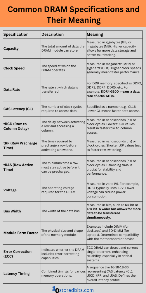
Understanding common DRAM specifications
Whenever you buy a DRAM for your computer, you will come across multiple specifications. Below are all of them and their purposes.
Frequently Asked Questions
What is the difference between DRAM and SRAM?
Unlike DRAM, SRAM doesn’t require constant refreshing because it is based on transistor memory instead of capacitor memory.
What is DRAM latency?
Latency refers to the delay between a memory request (read or write) and the time when the data is available. CAS latency is the time between sending a column address and when the data is available. rRCD or Row to column delay is the delay between activating the row and accessing the column. Row percentage time, or tRP, is the time it takes to precharge a row before the next row can be activated.
What is the difference between SDRAM and DRAM?
SDRAM is known as Synchronous DRAM, which operates in sync with the CPU’s clock. This allows the SDRAM to work more closely and uniformly with the CPU. However, the Asynchronous DRAM has its own clock,k which is generally slower and not in sync with the CPU. This results in slower performance compared to the SDRAM







You made everything so clear! I’ve learned a lot from it thanks to you!
Glad to hear!
Edit in Row Hit in DRAM section
It must 200 instead of 100
Let’s say DRAM accesses row 200, column 8. If the next memory access is also from row
100,200 (regardless of the column), it’s a row hit. This means DRAM doesn’t need to close the row and re-open it, speeding up the operation.please clarify.
Thanks, great explanation!
You are right. Thanks for picking the mistake out. It has been corrected.
Very good explanation, but DRAM normally does not refresh itself every 64ms.
It needs a self refresh command every few µs, to refresh a row.
If you have like 8192 rows, you need a self refresh every 7.8µs to refresh all 8192 rows within 64ms.
Trfc, refresh cycle time, which a refresh takes, is very quick, a few 100ns.
Auto refresh is only during DRAM standby, it does refresh internally then, but you can’t do any R/W operations, then.