Affiliate Disclosure: This post may include affiliate links. If you click and make a purchase, I may earn a small commission at no extra cost to you.
When searching for an SSD or flash drive, people often encounter various NAND Flash technologies and are unsure which one to choose. Most buyers are quite aware of the cell structure, i.e., SLC, MLC, TLC, and QLC, and which one is best for them. In the modern consumer market, we generally have two options to choose from: TLC and QLC. However, there are underlying technologies that power these memory cells and, consequently, the SSDs. They decide how the memory cells are organized to enhance performance, endurance, and capacity.
To provide context, 2D NAND is an older NAND Flash technology, whereas 3D NAND is the latest variant, featuring numerous improvements, the most important being vertical organization of cells. The V-NAND is a marketing term used by Samsung to describe its 3D NAND technology for SSDs. So, you can say that 3D NAND and V-NAND are the same. 2D and 3D NAND also use different types of memory cells, i.e., floating gate (in 2D NAND) and Charge Trap Flash (in 3D NAND).
The 2D NAND was highly successful in memory devices between the 1990s and 2000s, overcoming the issues with the earlier technologies, such as hard drives. However, there were serious scaling issues with this planar type of NAND flash. 2D NAND is called 2D because the memory cells are laid out in a planar structure, which makes it hard to scale.
There are several other differences between 2D and 3D NAND flash, which we will discuss in this article today. So, let’s get started.

What is 2D NAND Flash?
In the NAND Flash technology, the data is stored in the form of an electric charge (to represent the bits) inside the memory cells. In 2D NAND Flash, specifically, these memory cells are composed of floating gate transistors.
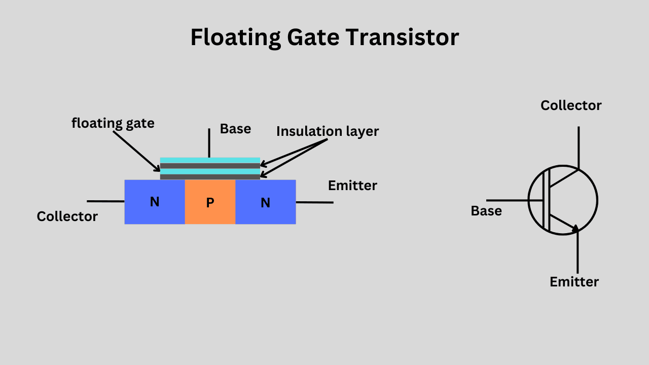
To create a full-fledged storage medium, millions or even billions of cells are required, depending on the total storage capacity. In 2D NAND technology, engineers arrange these cells in a flat, single-layer structure. Initially, it was sufficient to achieve good enough densities, but as demand for more storage space increased, this flat layering became a hindrance. The main reason wasn’t actually the flat plane structure but the inter-cell interference that happened due to the floating gate transistors. These transistors leaked a lot of charge and impacted the nearby cells.
In the image above, you can see that an insulation layer surrounds the floating gate, where the charge is stored. As the cells get smaller, the oxide layer becomes thinner, reducing its effectiveness and making it more prone to wear out or leakage.
How does 2D NAND Flash work and store data?
The floating gate transistor is the basic storage unit inside the 2D NAND, commonly referred to as a memory cell. The presence or absence in this memory cell represents the binary bits. There are three types of operations happening in the flash cells.
Program, Erase, and Read Operations
Programming a cell means injecting electrons inside the floating gate through the process of Fowler-Nordheim (FN) tunneling. Generally, when a cell is programmed (SLC), it represents a bit value of “0”. However, erasing the cell means the electrons are removed from the floating gate, and it represents the bit value “1”. To read the data from a cell, the control gate receives a voltage. The bit value is determined by the resulting current flow, which defines the threshold voltage shift by the stored charge. In SLC NAND cells, there will be just two threshold voltages and discrete charge levels, i.e., “low and high”. However, in the case of MLC, TLC, and QLC, the number of bits is more than one, and so are the discrete charge levels and hence the threshold voltages.

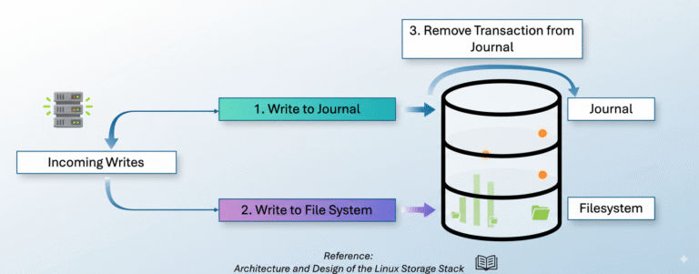
In any NAND flash, pages are the smallest writable unit (typically 4KB or 8KB) while blocks are made up of multiple pages (often 64 to 256 pages per block). The smallest programmable unit in NAND flash is a page, while the smallest erasable unit is a block.
2D NAND Architecture
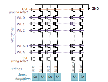
The architecture of 2D NAND is organized in a large matrix of memory cells connected in serie,s which forms a NAND string. Multiple strings are connected to form bit lines, and bit lines are combined to create a block.
Horizontal control lines connected to the control gate of memory cells are referred to as word lines. They are used for selecting rows of cells for read/write/erase. Vertical lines that connect to sources and drains of the transistors in a column are called the bit lines. A series of cells (generally 32 to 128 cells) connected in a series is called a NAND string. Additionally, each NAND string has a select transistor that connects to the source line. Also, there is a drain select transistor that connects to the bit line. These select transistors allow and disallow the control access to the memory cells. Here is a simplified diagram of a NAND block to help you understand its connections and basic operation.
Pros and Cons of 2D NAND
2D NAND isn’t a very popular storage technology in any storage space, but still, it has its benefits. The first benefit is that, due to its simple design, the manufacturing cost is lower than that of 3D NAND. It is a mature technology that has been tried and tested; however, due to today’s demands, its trends are fading away. It has a lower power consumption and also a simpler fabrication process.
If we discuss its drawbacks, the first one is that it is challenging to scale significantly due to cell-to-cell interference and charge leakage. The next problem is that it is hard to use in high-density storage drives. The endurance is low, and so is the performance. Additionally, as we attempt to scale this technology, the price per bit increases compared to the low storage densities.
What is 3D NAND Flash?
3D NAND Flash is the latest and most popular NAND flash technology, offering higher performance and storage density, while maintaining a nearly identical physical footprint to 2D Flash. The 3D NAND flash uses charge-trap flash memory cells instead of floating gate transistors. The charge-trap flash is a different variation of the transistor-based non-volatile memory, which uses a non-conductive material (usually Silicon Nitride) to hold the charge in place. It has a better charge-holding capacity compared to the floating gate. This property enables scaling to be even easier. 3D NAND has a different structure where the memory cells are spread both vertically and horizontally. This allows for better parallel processing but makes the circuitry much more complex.
With the help of TLC and QLC NAND flash using the 3D NAND, we are now seeing drives with pretty high storage capacities, such as 4TB and even 8TB. Here is a great resource to understand the practical implementation and the architecture of 3D NAND Flash using the CTF technology.


Also, since 3D NAND scales vertically, the cells can be larger compared to the ultra-small cells in 2D NAND. 3D NAND also offers numerous benefits with the latest etching techniques, as it does not rely heavily on extreme lithography.
How does 3D NAND Work and store data?
The main difference between the 2D and 3D NAND is the vertical stacking of memory cells into multiple layers (typically from 32 to over 200 layers). In the 3D NAND, the cells are organized in a vertical string structure (3D Pillar structure). A NAND string has multiple memory cells connected in series within a vertical column.
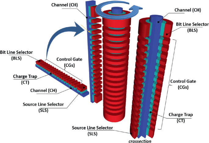
The horizontal control lines connecting to the control gates are referred to as wordlines. However, the vertical lines connecting to the source/drain of the cells in a string are called bitlines. The bitlines handle the data transfer during read/write operations, while the wordlines control these read/write operations.
Programming, Reading, and Erasing the Data
Again, the data is stored in the form of a charge, but this time, it will be kept in the charge-trap flash inside of a floating gate. They trap the electrons or program a memory cell, and a high voltage is applied to the control gate while the bitline and wordline of the same page are active. The process of injecting the electrons is again the Fowler-Nordheim (FN) tunneling. The trapped electrons will change the threshold voltage, which will then determine the bit value inside the cell. Similar to 2D NAND, multi-level cells (MLC, TLC, and QLC) utilize multiple voltage levels to represent multiple bits in a single cell.

To read the data, a small voltage is applied to the gate, which allows the current to flow through the channel. The amount of this current flow is measured to determine the bit values. If there is a charge stored inside the charge-trap layer, the threshold voltage increases and the cell requires more voltage to conduc,t indicating the logic state “0”.
To erase the data or to remove the trapped electrons, a negative voltage is applied to the control gate. This pulls the charge electrons inside the charge-trap layer out through the channel bank to the main substrate. Erasing a cell means returning the cell to its original threshold, which then represents the bit value of “1”.
Over time, this data tends to leak out of the cells in both 2D and 3D NAND. However, 3D NAND using the Charge-Trap rather than the floating gate is much more effective in holding the charge. Additionally, the cell size is larger in the 3D NAND, which contributes to improved overall data retention.
The architecture of 3D NAND
Vertical NAND String: Multiple memory cells connected in a vertical column make up a string. These strings are organized into blocks and pages.
Wordlines: Wordlines are horizontal lines connecting to the gates of the memory cells in each layer. Also, wordlines are shared across vertical layers for parallel operations.
Bitline: Bitlines are connected vertically to the source/drain of the cells in the vertical strings. The bit line is responsible for allowing data to be read and written.
Select Gate: At the top and bottom of each vertical string, select gates are used to control access for reading, erasing, and programming of the cells.
Pros and Cons of 3D NAND
The primary advantage of 3D NAND is its ability to scale and achieve extremely high storage densities. With 3D NAND, the areal density increases more than 10 times compared to 2D NAND, mainly due to the improvements in stacking layers and footprint scaling. Early 3D NAND implementations began with 24 layers, and modern devices have surpassed 200 layers. 3D NAND has higher endurance because the cell size is larger, allowing the dielectric insulator layer to be larger as well. This results in lower cell-to-cell interference and less charge leakage.
3D NAND has faster raw read/write speeds compared to 2D NAND because of the reduced interference and optimized architecture. Also, the power consumption is lower.
The biggest drawback of the 3D NAND is its high manufacturing cost, which can be overcome with time, but it is expensive than the 2D NAND. The extra processes for precise etching, stacking layers, and alignment of different layers make it a complex process. The die size is bigger because of the vertical stacking, which doesn’t affect much, but can show issues in the integrated devices, where space is a critical element. 3D NAND can be more sensitive to temperature changes, particularly in high-density designs such as TLC (Triple-Level Cell) and QLC.
What is Samsung’s V-NAND?
Samsung’s V-NAND is another name for 3D-NAND, marketed by Samsung in its Solid State Drives. The key difference with Samsung’s V-NAND is that it has increased the number of layers, reaching up to 290 layers.
With the 6th generation V-NAND, Samsung has reduced the cell size by up to 35% compared to the standard 3D NAND. Samsung employs advanced manufacturing techniques, utilizing a technology called channel-hole etching for NAND Flash, which enables the creation of multiple layers of billions of interconnected cells simultaneously. The latest V-NAND comes in a double-stack structure, which allows for a high layer count without significantly increasing the layer count. Samsung has made numerous other improvements to enhance performance and improve I/O functions.
Does V-NAND work just like the normal 3D NAND?
The working principles of both 3D NAND and V-NAND are the same. However, V-NAND offers faster read/write times due to the greater space between cells (vertically).
Both technologies write data by trapping electrons in a floating gate or charge trap (only charge trap in modern NANDs). When data is written, the voltage threshold is altered to represent stored bits. Now, just like the 3D NAND, V-NAND can be modified from SLC to MLC, TLC, and QLC.
In both 3D NAND and V-NAND, data is read by applying a voltage to determine the charge stored in the cells, which represents the data (0s and 1s). Both work on the principle of sensing the charge differences in the memory cells. Samsung claims that it has a much more efficient writing process, and with the vertical arrangement in V-NAND, lower program/erase voltages are required.
Resources:
https://arxiv.org/pdf/1807.05140
https://ieeexplore.ieee.org/abstract/document/9779282
https://www.mdpi.com/2073-431X/6/4/28
https://borecraft.com/files/kim2017.pdf
https://www.simms.co.uk/Uploads/Resources/50/f4366381-b992-425a-bec4-cca409b51a6c.pdf
https://link.springer.com/chapter/10.1007/978-3-031-03841-9_5
Nice post. I learn something totally new and challenging on websites
I am glad you liked it.
Thank you for the information. It helped me a lot.
Glad you liked it.