Affiliate Disclosure: This post may include affiliate links. If you click and make a purchase, I may earn a small commission at no extra cost to you.
SSDs retain data without power due to a unique phenomenon in electronics called charge trapping. The most basic storage element inside an SSD is a floating-gate MOSFET, also known as a Cell. With the help of microfabrication, millions of these floating-gate MOSFETs or charge-trap flash cells are embedded inside tiny NAND Flash chips.
Normal transistors do not retain the charge, but floating gate transistors can. Depending on their state, we can interpret it into the form of data.
When we combine millions and billions of these cells or transistors, we create NAND Flash memory. Now, because one floating gate transistor or cell can hold the data, the whole NAND Flash chip can hold all its data. In this way, the data is retained in the form of an electric charge, bit by bit, inside tiny cells. In 3D NAND, the cells are stacked vertically to increase storage density even more than 2D NAND.
Computers work with the help of digital data, which means the information must be in logic “0” and “1”. More precisely, the data must be stored using a series of high and low voltage levels. You can imagine the SSDs as huge circuitry that can be programmed or erased per our requirements.
Storing data inside an SSD is akin to programming this circuit with different voltages and then utilizing them for the interpretation of information. Each cell can hold 1, 2, 3, or 4 bits of information. So, it is a big but microscopic group of cells that always has some current, even if you have your drive unplugged from the computer.
How is data stored inside an SSD?
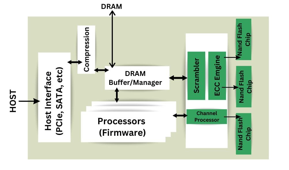
There are many different parts in an SSD. The main components include the controller, DRAM, Capacitors, Resistors, PCB, and NAND flash. The Controller is like the processor that takes the commands from the computer. RAM is there to keep the fast incoming flow of data in check and also to create tables of the data location on the NAND Flash. The real magic of permanent storage happens inside the NAND Flash. Older SSDs used floating gate, but as we switched to 3D NAND, we also switched to charge-trap flash.
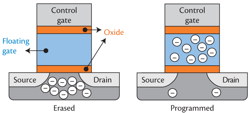
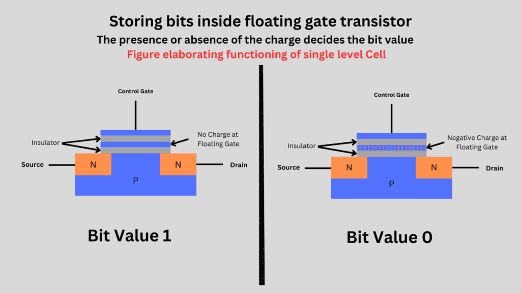
Now, to understand how this data retention happens, you’ll have to know a little about the workings of these floating gate transistors. Normal transistors can’t store current because there is no space for that. Floating-Gate Transistors and charge-trap cells have an extra layer of metal insulated by a dielectric material. Electric charge can be stored inside this layer. The dielectric prevents data from leaking out of this conductive layer, thereby enabling the data to remain there for extended periods.
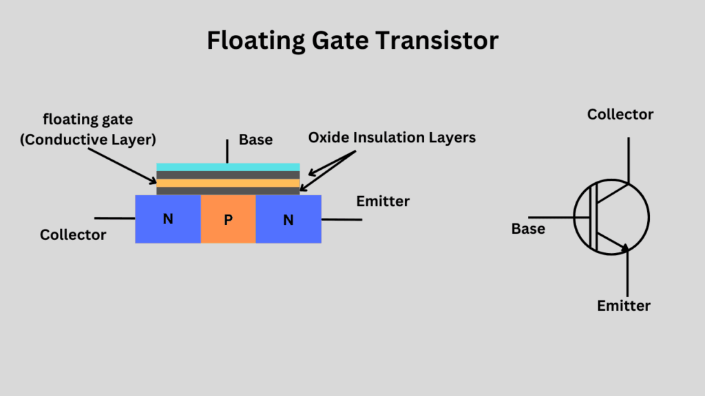

The controller takes the incoming data and programs each cell with either 0 or 1, i.e., high voltage or low voltage. When a high voltage is applied to the floating gate, the threshold voltage of the transistor changes. This threshold voltage can then be used to read the data.
All this happens at a very tiny scale, and to understand it in complete detail, you’ll have to dig a little deeper into the concepts of semiconductors and quantum physics.
But, in simple words, we combine millions and billions of these transistors inside semiconductor chips. If we store one bit per cell, we refer to it as an SLC SSD. For 2 bits per cell, we have MLC SSD, and so on. However, the fundamental thing is that we combine these cells to create ample space for storing these bits.
We work with numbers, alphabets, images, videos, etc, on our computers, but computers just understand 0s and 1s. So, even the very complex software and huge videos are working with 0s and 1s. This all needs storage, and because the scale of these numbers becomes so huge, we need very dense storage mediums. SSDs fulfill this demand because we are capable of fabricating billions of transistors inside tiny chips.
Floating Gate Transistor and its role in storing data without power requirements

Normal transistors can be utilized as switches or amplifiers in electronics. But various other types of transistors are there with different applications. A floating gate transistor is one of those. A normal transistor looks like this.

In a floating gate transistor, there are three additional layers: one floating gate and two insulating layers. This floating gate is where all the data storage happens. It can store a minimal amount of charge for years. In SSDs, this charge is utilized to store the information. A floating gate transistor looks like this.

Once a cell is charged with an appropriate charge level, the insulation layers around the floating gate prevent the charge from leaking. When we have to read the data, we just check the threshold voltage of the transistor. If it is higher than usual, then a charge on the floating gate has increased this voltage. The controller interprets it
Charge trapping and data retention.
Just look at a single cell. We have a cell that can be used to store a bit of data. It could be either 0 or 1. Just combine many of these cells, and you can store a series of bits that can be interpreted into the information the computer can utilize for doing things.
A significant amount of power is required when writing data to any SSD. The peak power consumption in high-speed Gen 5.0 drives can reach approximately 20 watts at times. However, once the charge is stored inside the NAND Flash, it remains there even if you unplug your drive from the computer.
Charge Leakage and its impact on data retention
Charge leakage is a real phenomenon in electronics. The insulating material that holds the charge inside the floating gate is fragile (in nanometers). Over time, this charge will leak to achieve an equilibrium. This is where hard drives tend to excel because they store data using magnetism.
The amount of charge leakage from the floating gate transistors increases as the SSDs age. Writing the data requires the charge to pass through this insulating material, which results in wear over time. So, if your drive is older, the chances of losing your data increase significantly.
Writing the data (in SLC SSD)
Imagine the host (CPU) issuing a command to write a chunk of data with the sequence of bits (1, 0, 1, 1) for permanent storage inside the SSD. The controller would take the request and locate the appropriate page, typically a 4KB (approximately 32,000 cells) page. It will first erase a block (comprising several pages), which will set all the cells to logic 1.
To write “1010”, the SSD will:
- Leave the first cell as “1” (no charge).
- Program the second cell to “0” (add charge).
- Leave the third cell as “1” (no charge).
- Leave the fourth cell to “1” (n charge).
The resulting state will be 1010.
For other types of SSDs like MLC, TLC, and QLC, multiple levels of voltages are utilized as thresholds and charge trapping to represent different bit levels. For example, a voltage zero can be used to store bit value 0-0-0 and voltage 0.1 as 0-0-1 and so on.
Reading the data (in SLC SSD)
Reading the data primarily involves locating the individual cells from the mapping table created during data writing. The controller sends the read voltage to the cells and checks the resulting current flow.
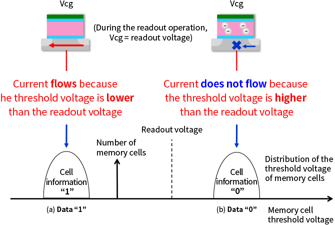
Consider reading the previously written binary data “1010” from a 4-cell page:
- Locate the Page: The controller identifies the specific page and accesses it.
- Apply Read Voltage: A read voltage is applied to the word line.
- Sense the State:
- Cell 1 (discharged, logical “1”): Current passes through easily.
- Cell 2 (charged, logical “0”): Current does not pass through easily.
- Cell 3 (discharged, logical “1”): Current passes through easily.
- Cell 4 (discharged, logical “1”): Current passes through easily.
The sense amplifiers detect the current flow and convert it to binary data: 1010. This is all done by the controller and at a swift pace, usually billions of operations per second.
How does SSD keep track of the data location?
We discussed that there could be billions of individual cells inside a single NAND Flash chip. So, as you can imagine, keeping track of the location of stored data is essential. While working on data in real-time, SSDs generally come with their own DRAM chips for creating the mapping tables. Even if it is a DRAM-less SSD, it would use the system’s RAM for creating these mapping tables.
These tables are then stored inside the NAND Flash itself for permanent storage. So, the data and its location are stored on the SSD itself.
The mapping tables do logical-to-physical address mappings. These tables ensure that the SSD controller knows the physical location of data on the NAND flash memory. The mapping could be done on the block level or page level, or sometimes, the OS can handle these operations as well.
Data retention periods in SSDs
In electronics, the simpler the design of a circuit or a component, the longer it tends to last. This is also true in the case of SSDs. There are three main types of NAND Flash memory cells used inside SSDs: SLC, MLC, TLC, and QLC.
SLC (Single-Level Cell) Flash Memory utilizes a single cell to store a single bit of data. It would either be 0 or 1. This makes the design more straightforward for the whole environment inside the drive. Generally, the SLC has the longest data retention period without power, i.e., 10 years or more.
MLC (Multi-Level Cell) Flash Memory uses a single cell to store two bits of data. The average data retention period without power is between 3 and 5 years.
TLC (Triple Level Cell) Flash memory uses a single cell to store three bits of data. The average data retention period without power is between 1 and 3 years.
QLC (Quad Level Cell) Flash memory uses a single cell to store four bits of data. This is a highly complex system that causes significant damage to cells within a relatively short timeframe. The average data retention period without power is between 1 and 2 years.
| NAND Type | Off-Power Retention @25–30 °C | After ~1 Year Use |
|---|---|---|
| SLC | ≥ 10 years (fresh) | 6–16 years (1K P/E) |
| MLC | ~5–10 years (fresh) | ≥ 10 years |
| TLC | ~3 years (fresh) | Decreases with wear |
| QLC | < 1 year (fresh) | Short (months) |
| 3D TLC | 1,500–5,000 P/E, retention similar to TLC (Wikipedia) | |
| 3D QLC | 100–1,500 P/E, retention lower than TLC (Wikipedia, Stored Bits) |


![The Best Disk Cloning Software of 2026 [Free/Paid]](https://storedbits.com/wp-content/uploads/2025/03/best-drive-cloning-software-768x432.png)

